Eureka AIR delivers breakthrough ideas for toughest innovation challenges, trusted by R&D personnel around the world.

Laser diode module for optical communication

Inactive Publication Date: 2006-03-28
SAMSUNG ELECTRONICS CO LTD
View PDF6 Cites 0 Cited by
  • Summary
  • Abstract
  • Description
  • Claims
  • Application Information

AI Technical Summary

Benefits of technology

[0015]The present invention is directed to a laser diode module for optical communication, which is a micro thermoelectric cooler capable of being installed through micro optical subassembly and reduces manufacturing cost.

Problems solved by technology

However, in regard to the conventional thermoelectric cooler, the plurality of pins are assembled manually and thereby results in manufacturing process complexity and high production costs, which makes it difficult to achieve a low cost laser diode module for optical communication.
Additionally, the thermoelectric cooler is too large in size to be installed through micro optical subassembly (OSA), such as a mini-plat requisite to optical transmitter / receiver (Tx / Rx) and a TO-can package, etc.

Method used


Image

  • Laser diode module for optical communication
  • Laser diode module for optical communication
  • Laser diode module for optical communication

Examples


Embodiment Construction

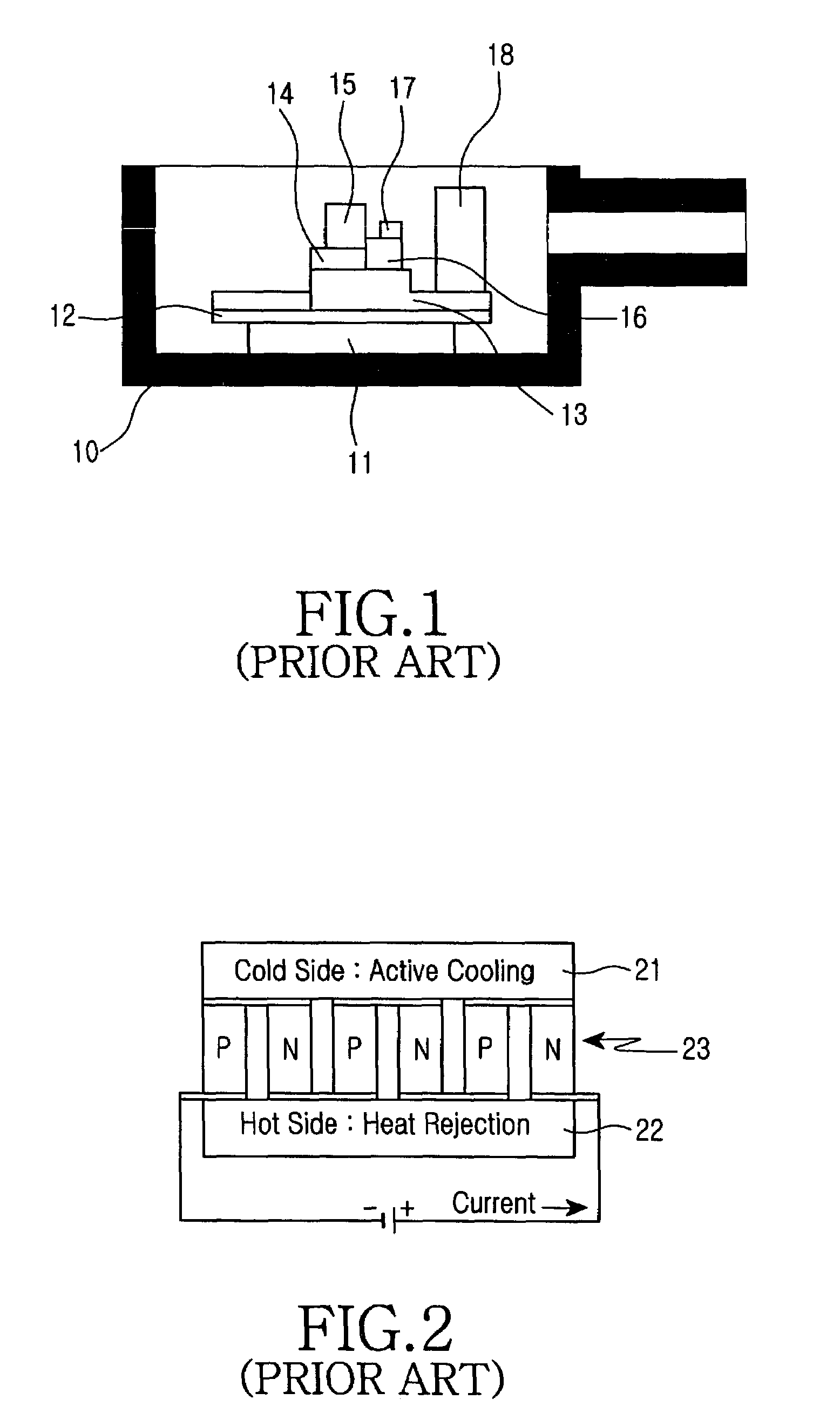
[0024]In the following description of the present invention, for purposes of explanation rather than limitation, specific details are set forth such as the particular architecture, interfaces, techniques, etc., in order to provide a thorough understanding of the present invention. However, it will be apparent to those skilled in the art that the present invention may be practiced in other embodiments that depart from these specific details. Moreover, it will be recognized that certain aspects of the figures are simplified for explanation purposes and that the full system environment for the invention will comprise many known functions and configurations all of which need not be shown here. In the drawings, the same or similar elements are denoted by the same reference numerals even though they are depicted in different drawings.

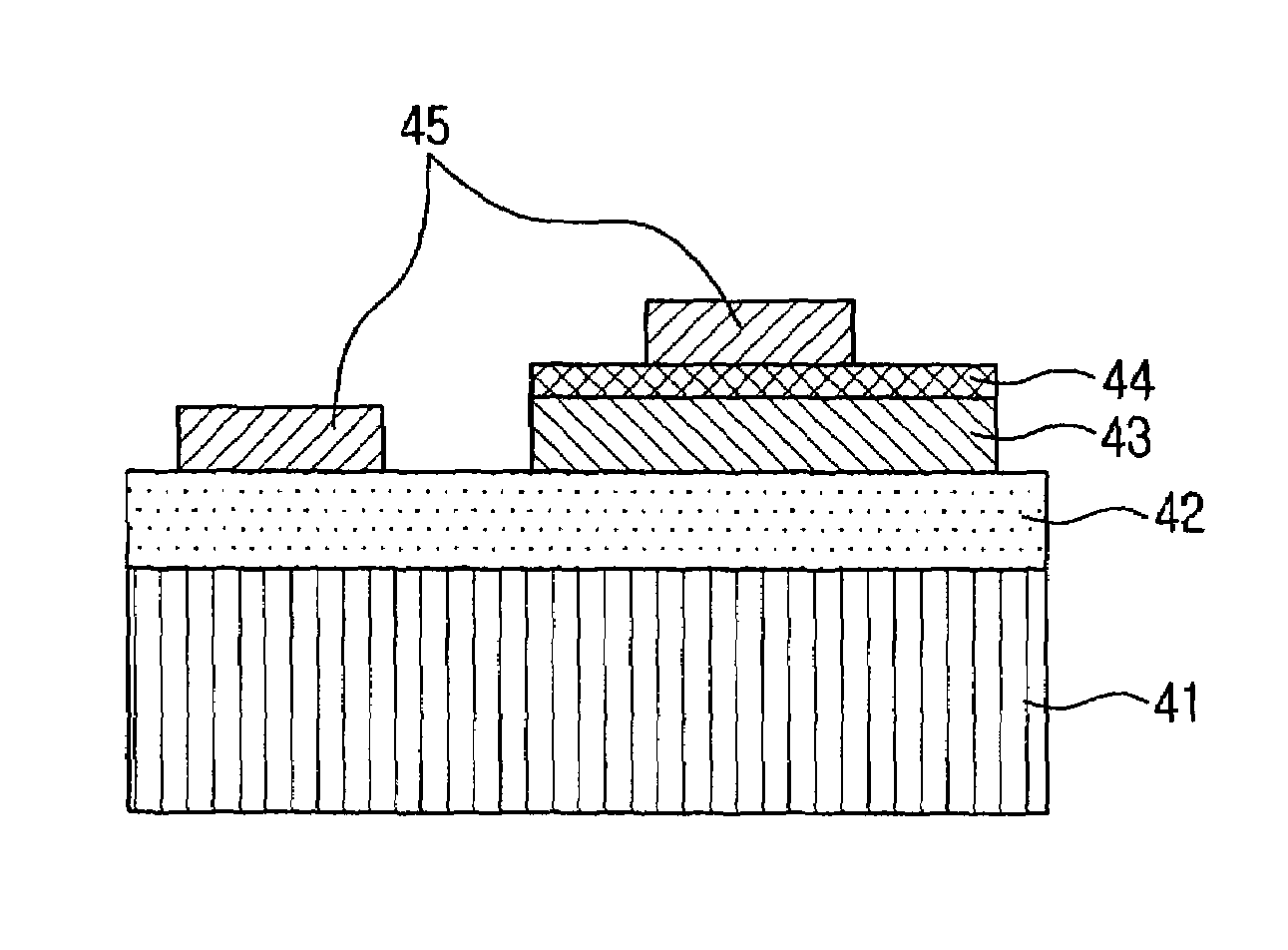
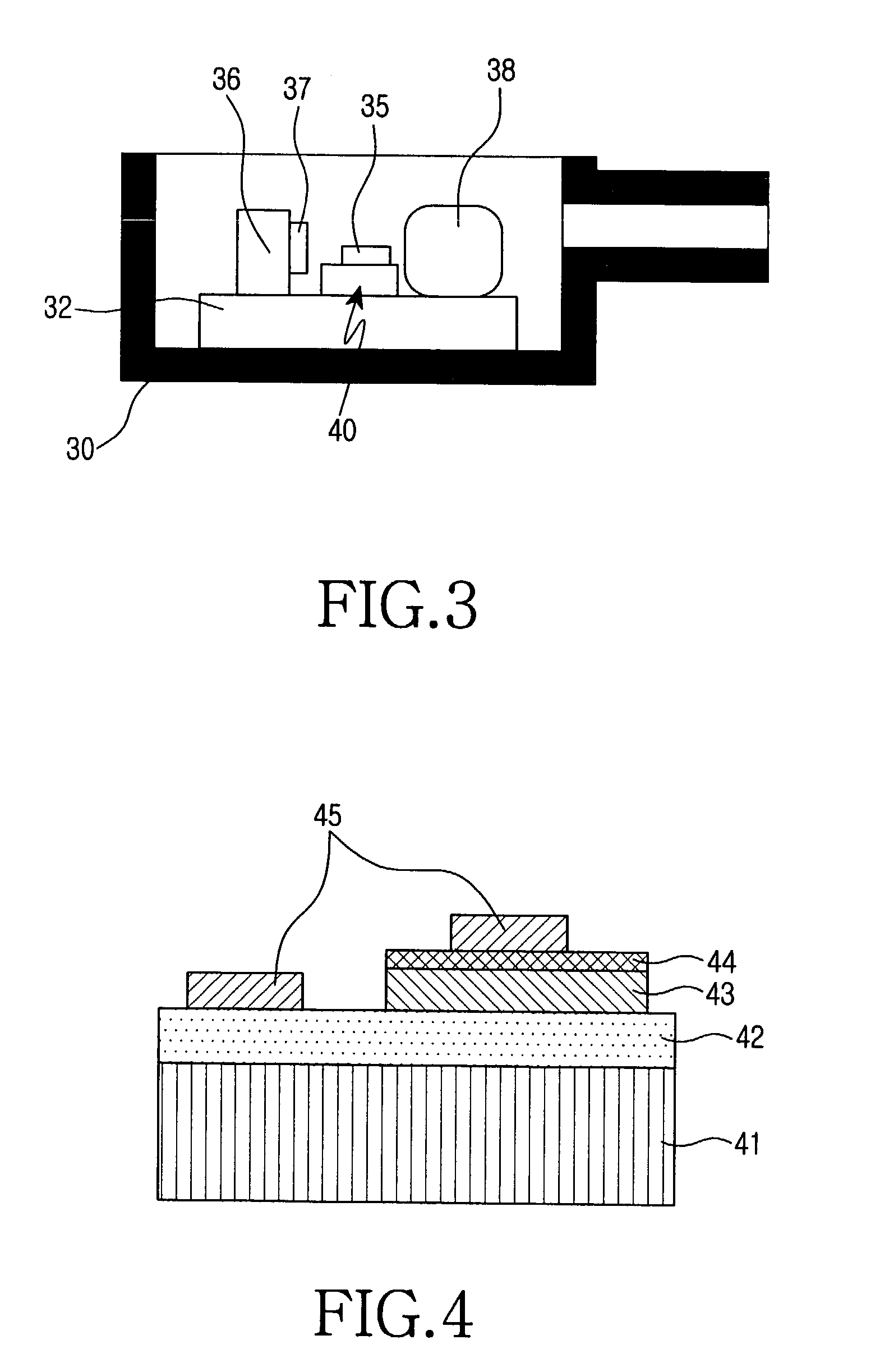
[0025]FIG. 3 is a schematic cross-sectional view of a laser diode module for optical communication in accordance with the principles of the present invention...


PUM


Abstract

A laser diode module for optical communication is disclosed and includes a plurality of leads, a housing having a vertical wall, a heat sink disposed on the housing, a superlattice microcooler disposed on the heat sink, a laser diode disposed on one side of the superlattice microcooler, a photo diode to convert the received light emitted from the laser diode into current, and a light condensing unit disposed on one side of the heat sink to condense the laser beams emitted from the laser diode.

Description

CLAIM OF PRIORITY[0001]This application claims priority to an application entitled “laser diode module for optical communication,” filed with the Korean Intellectual Property Office on Jan. 2, 2003 and assigned Ser. No. 2003-139, the contents of which are hereby incorporated by reference.BACKGROUND OF THE INVENTION[0002]1. Field of the Invention[0003]The present invention relates to a laser diode module for optical communication, and more particularly to a laser diode module for optical communication employing a superlattice microcooler.[0004]2. Description of the Related Art[0005]As is generally known in the art, a semiconductor laser device is made of a semiconductor device that is based on a P—N bonding structure and employs quantum electron concepts. In particular, a semiconductor laser diode emits light corresponding to reduced energies produced from the recombination of vacancies and holes. The recombination of vacancies and holes are induced intentionally by applying current ...

Claims


Application Information

Patent Timeline
IPC IPC(8): H01S5/00B81B1/00G02B6/42H01L23/38H01L31/167H01S3/04H01S3/091H01S5/02H01S5/022H01S5/024
CPCH01L31/167H01S5/02469H01S5/02248H01S5/02438H01S5/02476H01L2924/0002H01S5/0683H01L2924/00H01S5/02325G02B6/42
Inventor LEE, SANG-HO
Owner SAMSUNG ELECTRONICS CO LTD
Why Eureka
Eureka Blog
Learn More