Semiconductor device having crystalline semiconductor layer

a semiconductor layer and semiconductor technology, applied in the direction of semiconductor devices, electrical devices, transistors, etc., can solve the problems of hurried development of the switching element of the image display device, and the drive circuit is still far from the state of fully satisfying the required performance, and achieve the effect of high performan

Inactive Publication Date: 2006-04-04
SEMICON ENERGY LAB CO LTD
View PDF46 Cites 59 Cited by
  • Summary
  • Abstract
  • Description
  • Claims
  • Application Information

AI Technical Summary

Benefits of technology

[0013]It is conceivable, as a reason why a high performance TFT as mentioned above has not been able to be obtained by a conventional method, that carriers (electrons or holes) are captured by crystal grain boundaries so that improvement of an field effect mobility as one of parameters showing TFT characteristics has been prevented.
[0015]In order to realize a semiconductor device of the present invention, it is indispensable to provide a technique to change the structure of such “malignant crystal grain boundaries” into “benign crystal grain boundaries” for carriers. That is, it is important to form crystal grain boundaries which have a low probability of capturing carriers, that is, a low possibility of blocking the movement of carries.
[0031]The present invention provides a semiconductor device with high performance which can constitute a drive circuit or a logic circuit by using a crystalline silicon film having the structure as described above so as to form an active layer of the semiconductor device typified by a TFT.

Problems solved by technology

The thin film transistor is widely applied to an electronic device such as an IC or an electro-optical device, and especially, its development as a switching element for an image display device has been hurried.
However, even if a drive circuit is constituted by using such a TFT, the drive circuit is still far from the state of completely satisfying the required performance.

Method used


Image

  • Semiconductor device having crystalline semiconductor layer
  • Semiconductor device having crystalline semiconductor layer
  • Semiconductor device having crystalline semiconductor layer

Examples


first embodiment

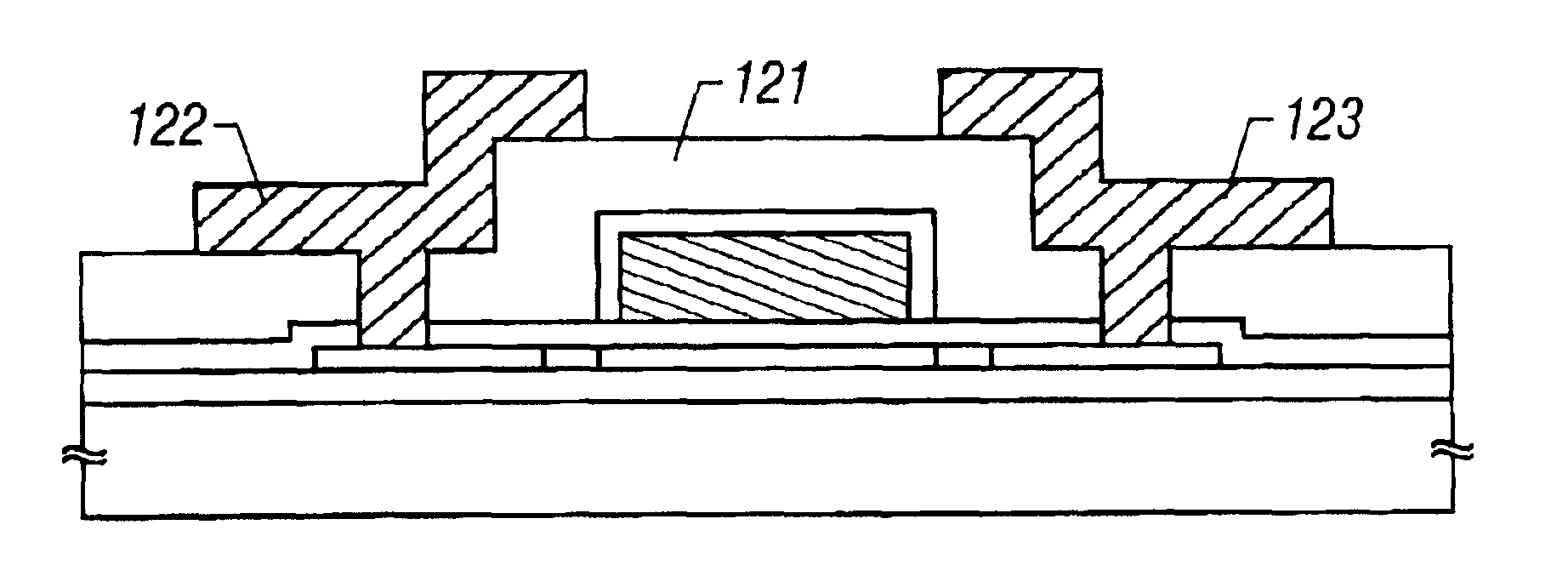
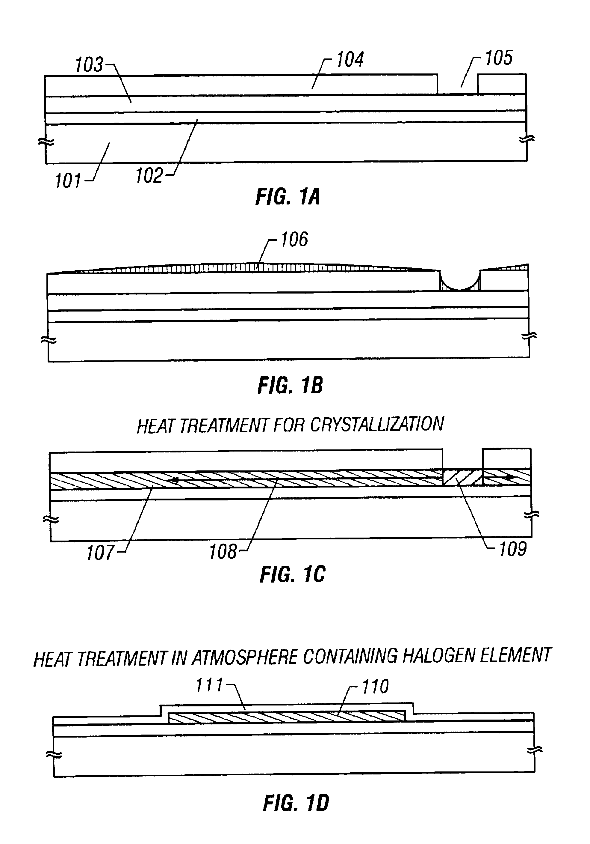
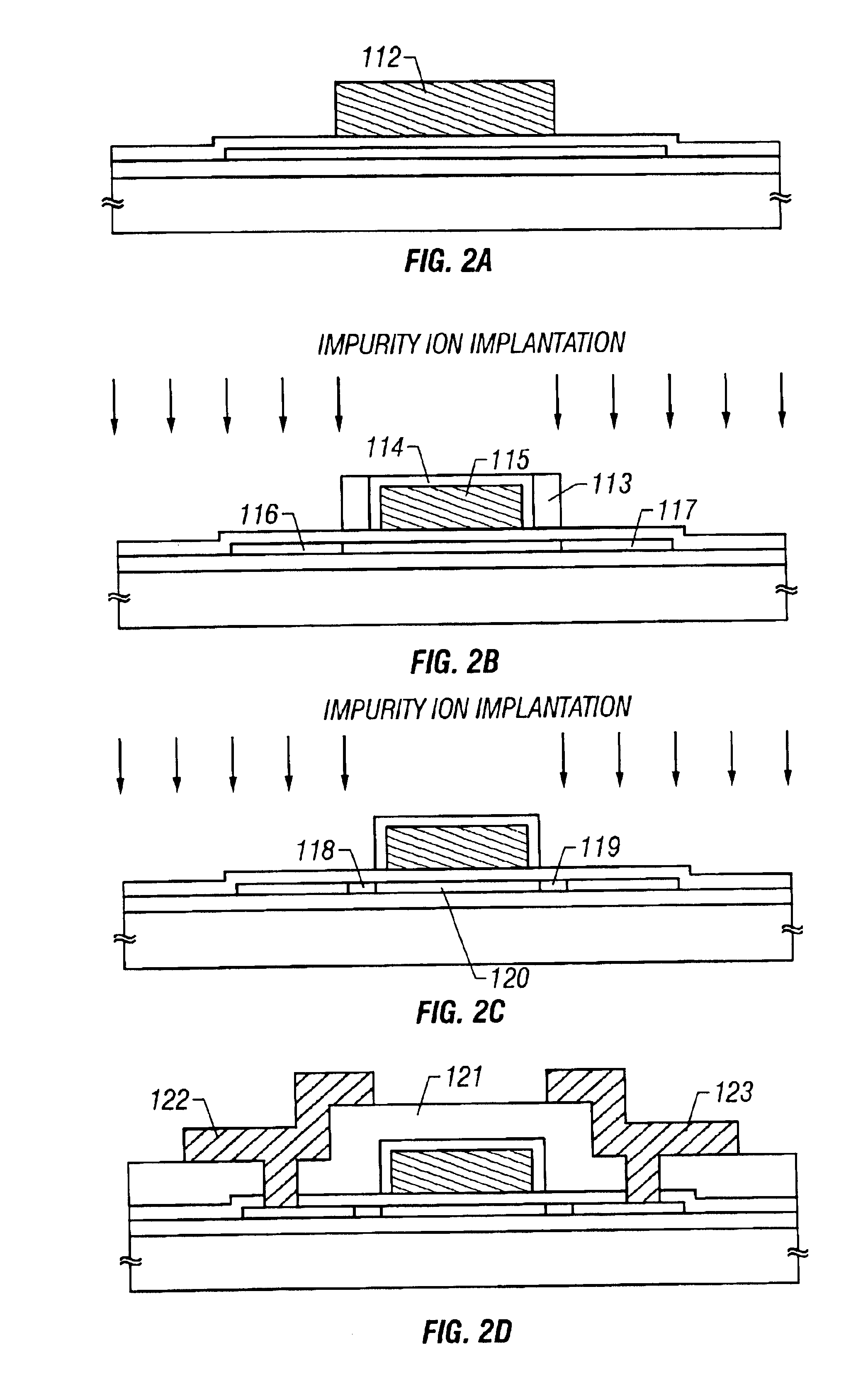
[0049][First Embodiment]

[0050]In this embodiment, there is described an example where a crystalline silicon film formed in accordance with a manufacturing method of the present invention is used as an active layer of a thin film transistor (TFT). FIGS. 1A to 1D show part of manufacturing steps of the TFT.

[0051]Incidentally, means for crystallizing an amorphous silicon film used in this embodiment is a technique disclosed in Japanese Patent Unexamined Publication No. Hei. 7-321339. Accordingly, in this embodiment, since only a brief description thereof will be disclosed, please refer to the publication for details.

[0052]First, a substrate 101 having an insulating surface is prepared. In this embodiment, a silicon oxide film 102 with a thickness of 2000 Å as an under layer is formed on a quartz substrate. A method of forming the silicon oxide film 102 includes a low pressure thermal CVD method, a plasma CVD method, a sputtering method and the like.

[0053]According to research of the pr...

second embodiment

[0152][Second Embodiment]

[0153]In this embodiment, a CMOS circuit is formed by a TFT shown in the first embodiment. The CMOS circuit is constituted by complementarily combining an N-channel type TFT and a P-channel type TFT having the structure as shown in the first embodiment.

[0154]Manufacturing steps of the CMOS circuit of this embodiment will be described with reference to FIGS. 5 and 6. The range of application of the crystalline silicon film formed by the present invention is wide, and the method of forming the CMOS circuit is not limited to this embodiment.

[0155]First, in accordance with the manufacturing procedure shown in the first embodiment, a silicon oxide film 502 is formed on a quartz substrate 501, and a crystalline silicon film (not shown) is formed thereon. By patterning the crystalline silicon film, an active layer 503 for an N-channel type TFT and an active layer 504 of a P-channel type TFT are formed.

[0156]After the active layers 503 and 504 are formed, a gate ins...

third embodiment

[0216][Third Embodiment]

[0217]This embodiment shows other manufacturing steps than those shown in the first embodiment. Specifically, prior to the formation of an active layer, a heat treatment in an atmosphere containing a halogen element is carried out to a crystalline silicon film to remove nickel through gettering.

[0218]By combining the step shown in this embodiment with the first embodiment, it is possible to further effectively decrease the nickel concentration in the active layer.

[0219]By the heat treatment over 700° C., the film thickness of the crystalline silicon film is decreased, so that this embodiment has also an effect to thin the active layer. If the film thickness becomes thin, it is expected that the mobility is improved and off-state current is decreased.


PUM


Abstract

A semiconductor device having performance comparable with a MOSFET is provided. An active layer of the semiconductor device is formed by a crystalline silicon film crystallized by using a metal element for promoting crystallization, and further by carrying out a heat treatment in an atmosphere containing a halogen element to carry out gettering of the metal element. The active layer after this process is constituted by an aggregation of a plurality of needle-shaped or column-shaped crystals. A semiconductor device manufactured by using this crystalline structure has extremely high performance.

Description

[0001]This is a continuation of U.S. application Ser. No. 08 / 951,819 filed Oct. 14, 1997 now U.S. Pat. No. 6,365,933BACKGROUND OF THE INVENTION[0002]1. Field of the Invention[0003]The present invention relates to a semiconductor device having an active layer of a semiconductor thin film formed on a substrate having an insulating surface, and particularly to a thin film transistor in which an active layer is made of a crystalline silicon film.[0004]2. Description of the Related Art[0005]In recent years, attention has been paid to a technique in which a thin film transistor (TFT) is constituted by using a semiconductor thin film (thickness of about hundreds to thousands A) formed on a substrate having an insulating surface. The thin film transistor is widely applied to an electronic device such as an IC or an electro-optical device, and especially, its development as a switching element for an image display device has been hurried.[0006]For example, in a liquid crystal display device,...

Claims


Application Information

Patent Timeline
Patent Type & Authority Patents(United States)
IPC IPC(8): H01L31/0392H01L21/20H01L21/336H01L21/77H01L21/8242H01L21/84H01L27/12H01L29/04H01L29/76H01L29/786
CPCH01L21/32055H01L21/321H01L21/3221H01L27/1277H01L29/04H01L29/66757H01L29/78621H01L29/78675H01L29/78696H01L27/12H01L21/02532H01L21/02672H01L27/10873H10B12/05H01L21/18
Inventor YAMAZAKI, SHUNPEIOHTANI, HISASHIKOYAMA, JUNFUKUNAGA, TAKESHI
Owner SEMICON ENERGY LAB CO LTD
Why Eureka
Try Eureka