Chip management system

a management system and chip technology, applied in the field of integrated circuit design, can solve the problems of inability to design complex chips, inability to meet the requirements of the design process, and the complexity of the design process has become so ubiquitous and widespread, and achieve the effect of increasing the design productivity

Inactive Publication Date: 2006-04-04
BELL SEMICON LLC
View PDF16 Cites 72 Cited by
  • Summary
  • Abstract
  • Description
  • Claims
  • Application Information

AI Technical Summary

Benefits of technology

[0010]According to the system and method disclosed herein, the present invention is implemented as a web-based expert system that increases design productivity by employing a metamethodology focused on design flow supported by third party EDA tools. The expert system provides a deterministic, unified user-interface that integrates the functions required to design and bu

Problems solved by technology

However, this has resulted in a level of design complexity previously unimagined.
The variety of such tools is supplied from a plurality of sources; this results in compatibility and management issues.
For instance, cost issues, the number of features to be included, and performance considerations all dictate the parameters desired in a chip by a consumer.
Designing complex chips has become so ubiquitous

Method used


Image

  • Chip management system
  • Chip management system
  • Chip management system

Examples


Embodiment Construction

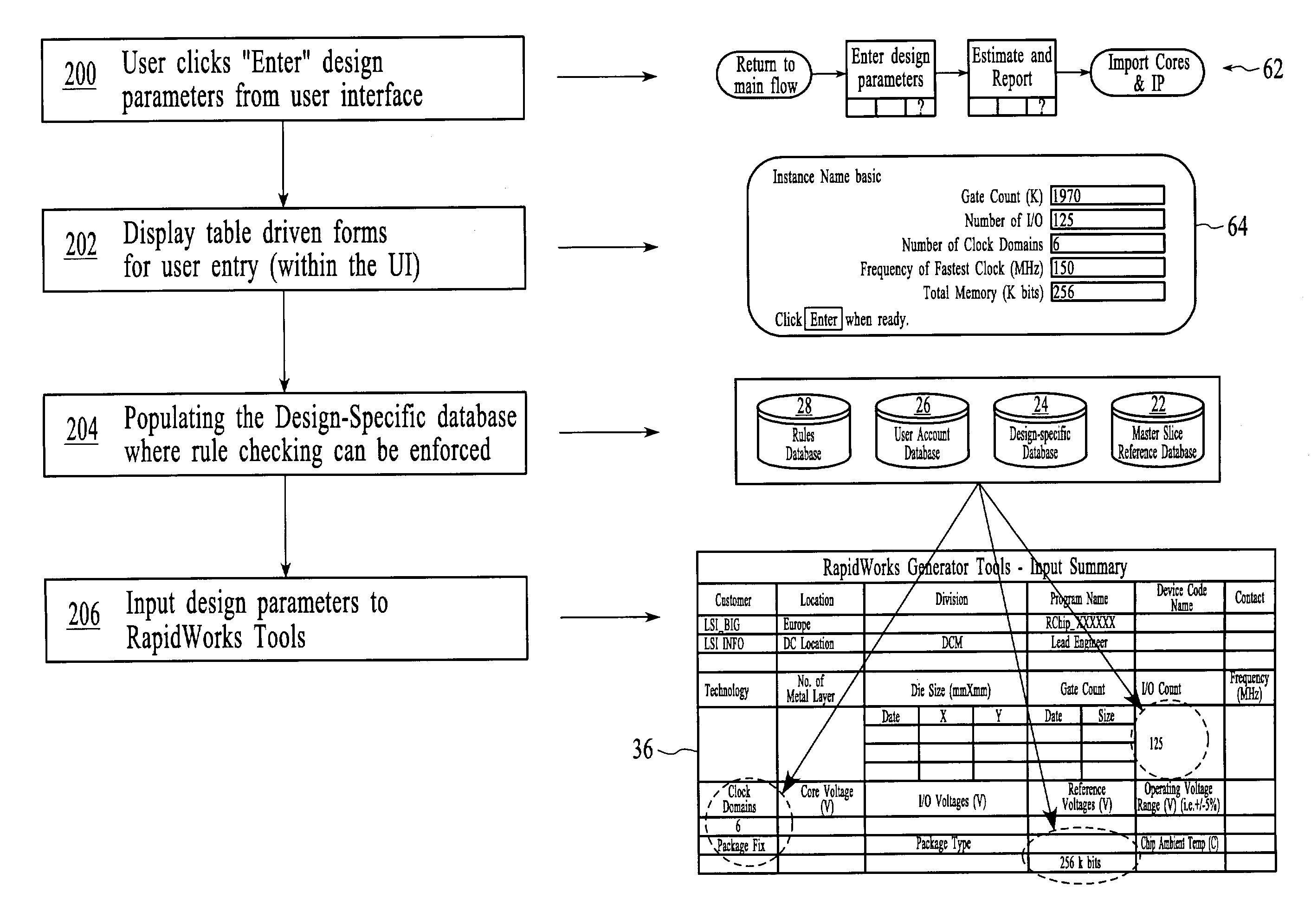
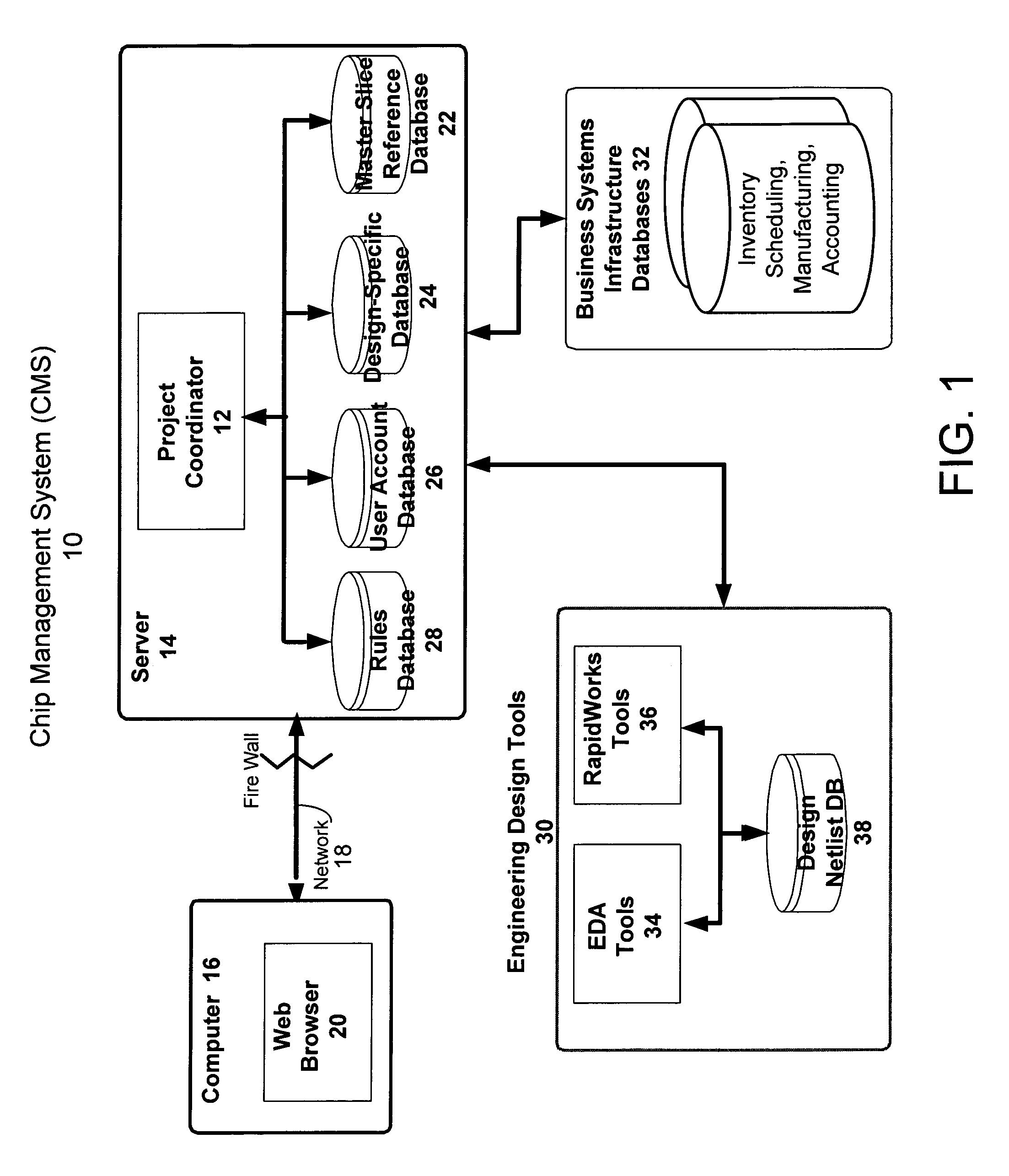
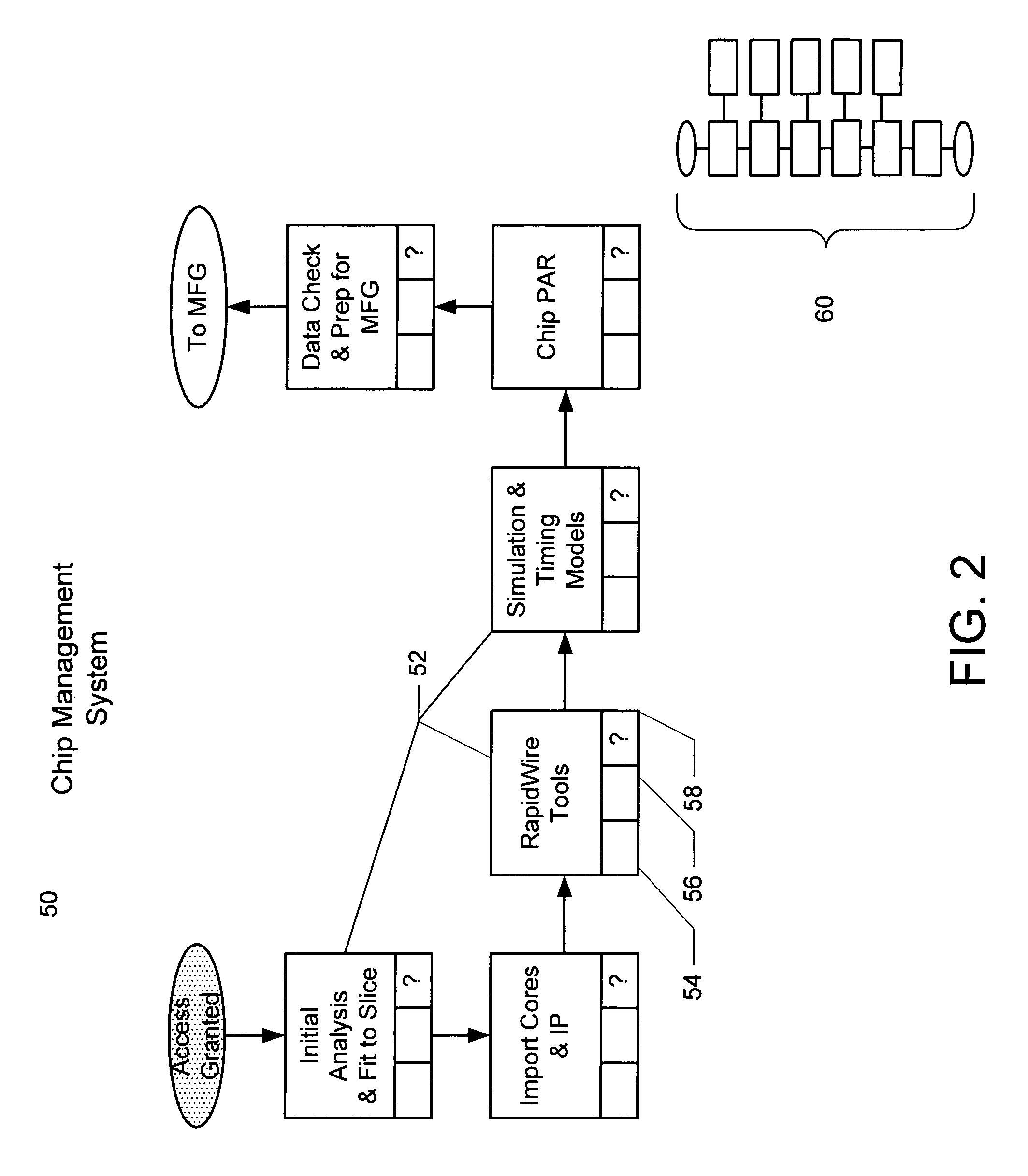
[0019]The present invention relates to automated design methodologies of integrated circuits. The following description is presented to enable one of ordinary skill in the art to make and use the invention and is provided in the context of a patent application and its requirements. Various modifications to the preferred embodiments and the generic principles and features described herein will be readily apparent to those skilled in the art. Thus, the present invention is not intended to be limited to the embodiments shown but is to be accorded the widest scope consistent with the principles and features described herein.

[0020]A fundamental problem resolved by the present invention is to provide a manufacturer with the ability to provide a wide range of IC products, by a wide range of designers to a variety of customers. For example, the present invention may provide a system to achieve actual variable semiconductor products, for example, field programmable gate arrays (FPGAs) applic...


PUM


Abstract

A method and system for automatically guiding a user through a design flow for an integrated circuit are disclosed. The method and system include displaying a design flow user interface on a user's computer, where the user interface includes symbols corresponding to design flow process steps. The design flow process steps are defined with a set of rules, and user input for each step is analyzed for compliance with the rules. The user is allowed to proceed to a next step in the flow once it is determined that the previous steps have been completed successfully.

Description

CROSS-REFERENCE TO RELATED APPLICATIONS[0001]The present invention is related to co-pending patent application Ser. No. 10 / 015,194 entitled “METHOD AND APPARATUS FOR IMPLEMENTING A METAMETHODOLOGY” filed on Nov. 20, 2001, by the assignee of the present application and included herein by reference in its entirety.FIELD OF THE INVENTION[0002]The present invention generally relates to the field of integrated circuit design, and more particularly to a method for automatically guiding a user through a design flow for an integrated circuit (IC).BACKGROUND OF THE INVENTION[0003]Integrated circuits have become a necessary part of everyday modern society. From cell phones and computers, to household appliances and automobiles, a wide range of integrated circuits are utilized to provide a broad range of functionality. To provide this functionality, integrated circuits may need to be specialized to have the functions necessary to achieve the desired results. Additionally, more and more functio...

Claims


Application Information

Patent Timeline
IPC IPC(8): G06F17/50G06F19/00G06F9/455G06Q50/00H01L21/02
CPCG06F17/50G06F17/5045Y10S706/921G06F2217/06G06F2111/04G06F30/30G06F30/00G06F30/31
Inventor WEED, DAN
Owner BELL SEMICON LLC
Why Eureka
Try Eureka