Programmable logic device

a logic device and programmable technology, applied in the direction of logic circuit coupling/interface arrangement, pulse technique, instruments, etc., can solve the problems of affecting the size and cost of equipment, affecting the power consumption of that part of the device, and performing a potentially lengthy configuration sequence, so as to reduce the voltage

Inactive Publication Date: 2006-04-11
ALTERA CORP
View PDF7 Cites 29 Cited by
  • Summary
  • Abstract
  • Description
  • Claims
  • Application Information

AI Technical Summary

Benefits of technology

[0012]While power is removed from some or all of the programmable active logic section of the device, while still being applied to the configu

Problems solved by technology

When a part of an integrated circuit device is connected to its power supply, there will always be some current leakage, using conventional technologies, and hence some power consumption within that part of the device.
In other cases, a high power consumption requires that the equipment be provided with special heat dissipating

Method used


Image

  • Programmable logic device
  • Programmable logic device
  • Programmable logic device

Examples


first embodiment

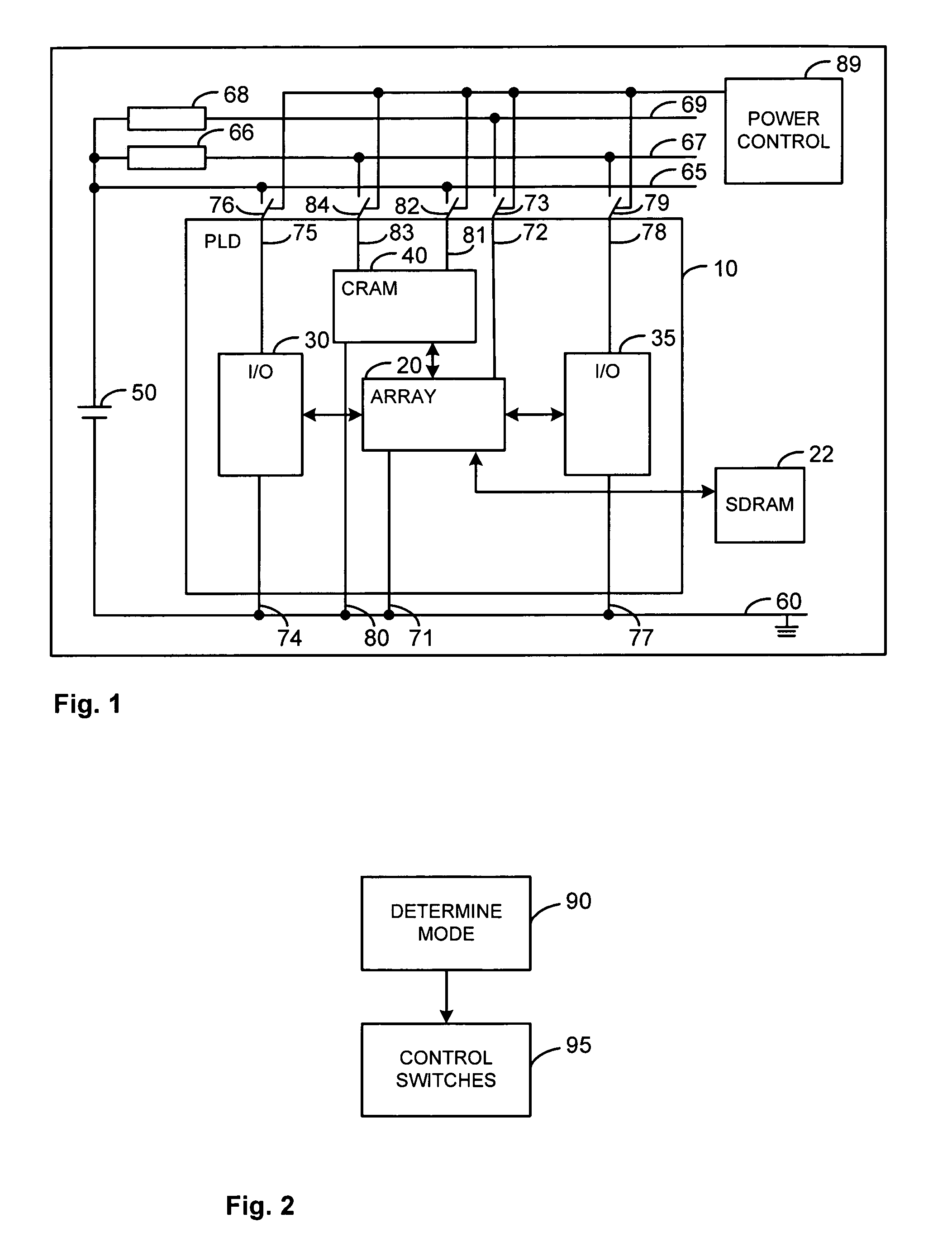
[0017]FIG. 1 shows a programmable logic device according to the invention.

[0018]As is conventional, the programmable logic device 10 is based around an active logic section in the form of a gate array 20, which is made up of programmable logic elements, plus the associated registers and other logic resources, as is conventional. The device 10 also comprises input / output blocks 30, 35, which connect the logic elements of the array 20 to the input / output pins (not shown) of the device 10.

[0019]Interconnections between the logic elements of the gate array 20, and between the logic elements and the input / output blocks 30, 35, are controlled by configuration data.

[0020]The function of the configuration data is to control these interconnections so that the device 10 performs its intended function. The configuration data is stored in a configuration memory (or configuration RAM, or CRAM) 40. The stored data can then be applied to the logic elements 20 and the input / output blocks 30, 35.

[00...

second embodiment

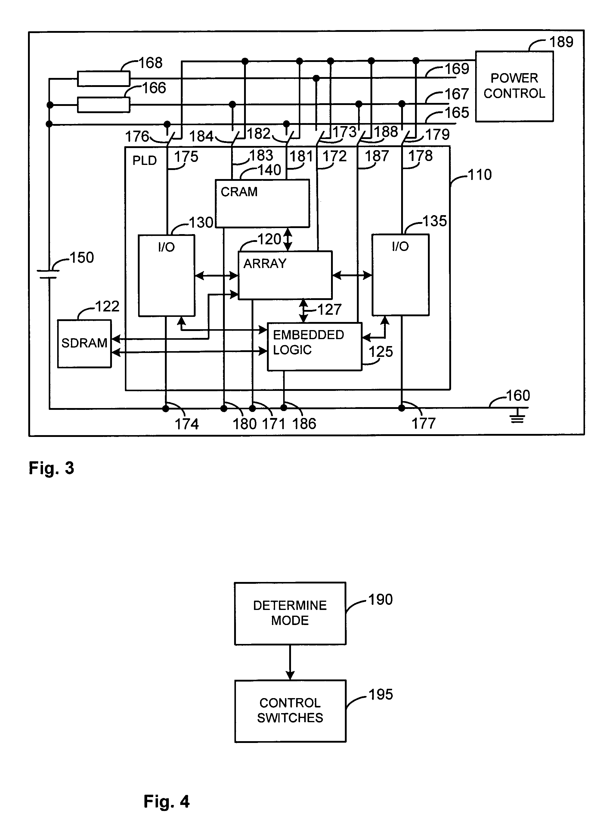
[0038]FIG. 3 shows a programmable logic device according to the invention.

[0039]Again, the programmable logic device 110 includes a gate array 120, which is made up of programmable logic elements, plus the associated registers and other logic resources. In this case, the active logic section of the device also includes an embedded logic block 125, which in a preferred embodiment of the invention includes an embedded processor and its associated registers, etc, which is provided to allow the device to perform specific processing functions more efficiently than can be achieved by a gate array alone. The embedded logic block may be programmable, or may be hard-wired to carry out specific functionality. The embedded logic block 125 is connected to the gate array 120 by means of an interface 127. The device 110 also comprises input / output blocks 130, 135, which connect the logic elements of the array 120 and embedded logic block 125 to the input / output pins (not shown) of the device 110....


PUM


Abstract

A programmable logic device is provided with multiple power supplies such that, in one mode of operation, power can be disconnected from at least one part of the programmable logic device, while maintaining power at least to an interface component of the programmable logic device, or to a memory component in which current configuration data are stored, thereby avoiding the need for a configuration sequence when power is reapplied to the whole device. The programmable logic device may be provided as an integrated circuit, having multiple pairs of pins for connection to a supply voltage. Each of the pairs of pins provides power for a different subsection of the programmable logic device.

Description

BACKGROUND OF THE INVENTION[0001]This invention relates to a programmable logic device (PLD) or field programmable gate array (FPGA). In particular, it relates to the implementation of a power source for the device.[0002]A programmable logic device is an integrated circuit, which includes a large number of logic elements, usually arranged in the form of an array. After manufacture, these logic elements can be combined, by programming the possible interconnections between the logical elements in a particular way, so that the device performs a particular desired set of functions.[0003]In order to allow the required interconnections to be made, the programmable logic device includes a routing structure. The routing structure allows communication between the different logic elements in the array.[0004]After manufacture of the programmable logic device, functions are allocated to the logic elements, and the interconnections between the logic elements are programmed, in such a way that th...

Claims


Application Information

Patent Timeline
IPC IPC(8): H03K19/177
CPCH03K19/17732H03K19/17784H03K19/17772
Inventor MAY, ROGERCROSLAND, ANDREWFLAHERTY, EDWARD
Owner ALTERA CORP
Why Eureka
Try Eureka