Cooling system for a semiconductor device and method of fabricating same

a cooling system and semiconductor technology, applied in semiconductor devices, semiconductor/solid-state device details, electrical devices, etc., can solve the problems of increasing chip area, reducing circuit density, and increasing chip area of known passive or active semiconductor cooling systems

Active Publication Date: 2006-04-18
GLOBALFOUNDRIES U S INC
View PDF13 Cites 96 Cited by
  • Summary
  • Abstract
  • Description
  • Claims
  • Application Information

AI Technical Summary

Problems solved by technology

However, many known passive or active semiconductor cooling systems are incapable of adequately dissipating excessive amounts of thermal heat.
For example, front-side trench etching results in increased chip area and reduced circuit density.
Another problem with front-side trench etching is that the trench must be relatively small due to the area constraints and deep enough to extend from the front side to the backside of a chip.
As a result, the processing of small and deep trenches is time consuming and expensive.
Front-side trench etching also can degrade device reliability.
Due to the close proximity of trenches to semiconductor devices on a chip, undesirable crystalline defects, such as dislocations, may result from mechanical stress caused during the fabrication of a trench.
Further, front-side trench etching may compromise the quality of a metal interconnect.
The etching of deep trenches through metal interconnect levels may force some metal wires to change their routing path and may reduce the density of the metal interconnects.

Method used


Image

  • Cooling system for a semiconductor device and method of fabricating same
  • Cooling system for a semiconductor device and method of fabricating same
  • Cooling system for a semiconductor device and method of fabricating same

Examples


Embodiment Construction

[0028]Preferred embodiments of the present invention will be described below in more detail with reference to the accompanying drawings. This invention may, however, be embodied in different forms and should not be construed as limited to the embodiments set forth herein. Rather, these embodiments are provided so that this disclosure will be thorough and complete, and will fully convey the scope of the invention to those skilled in the art.

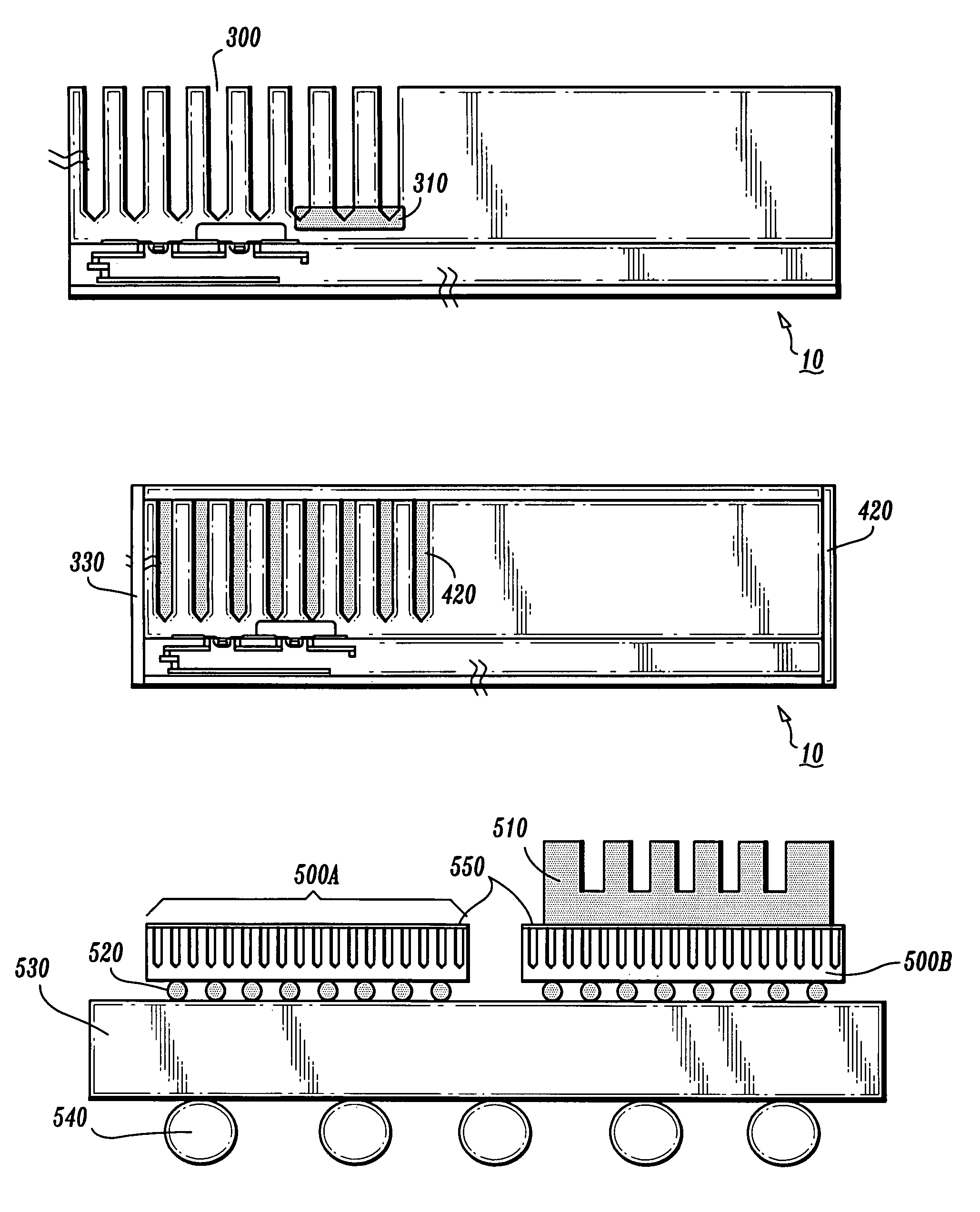
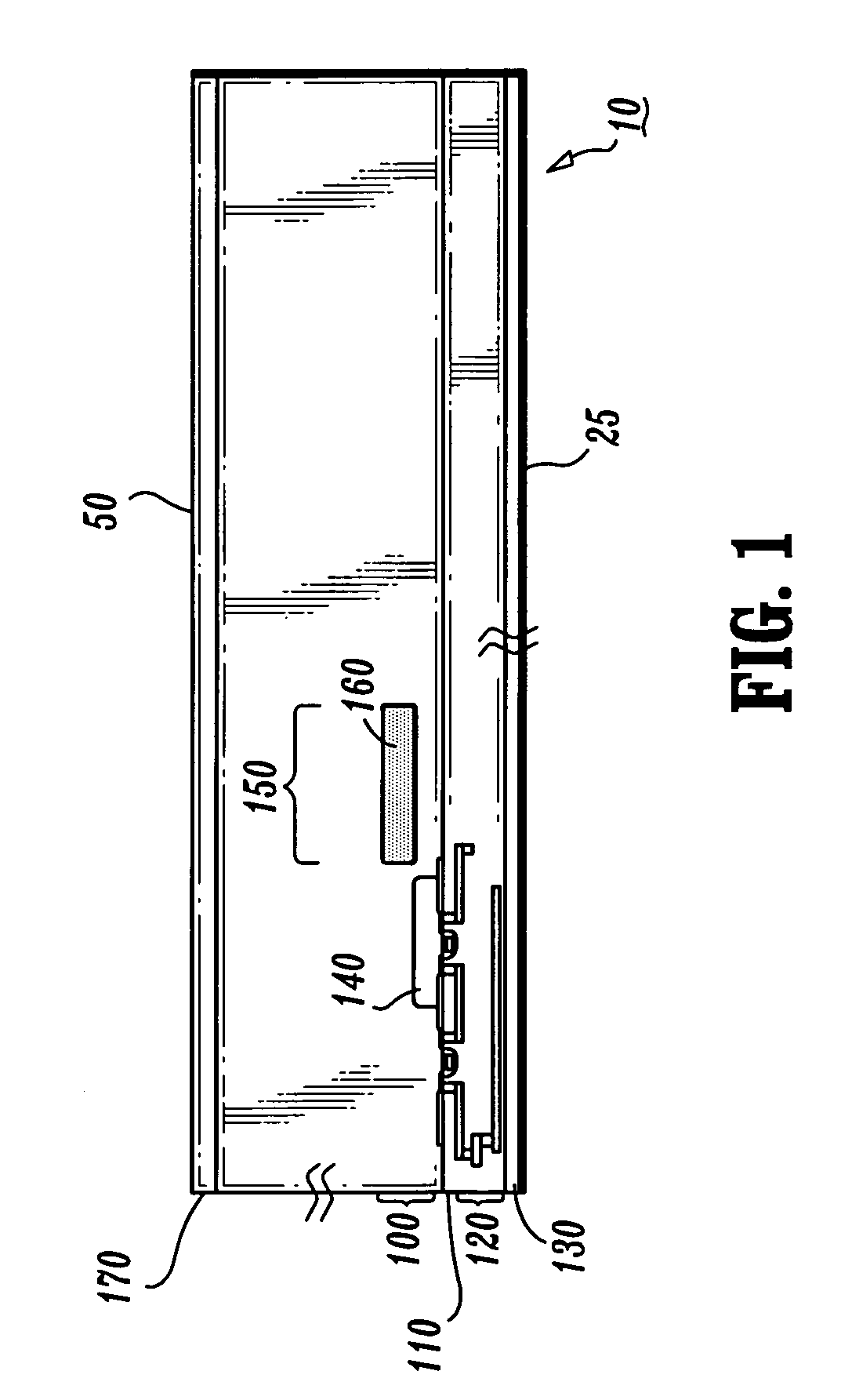
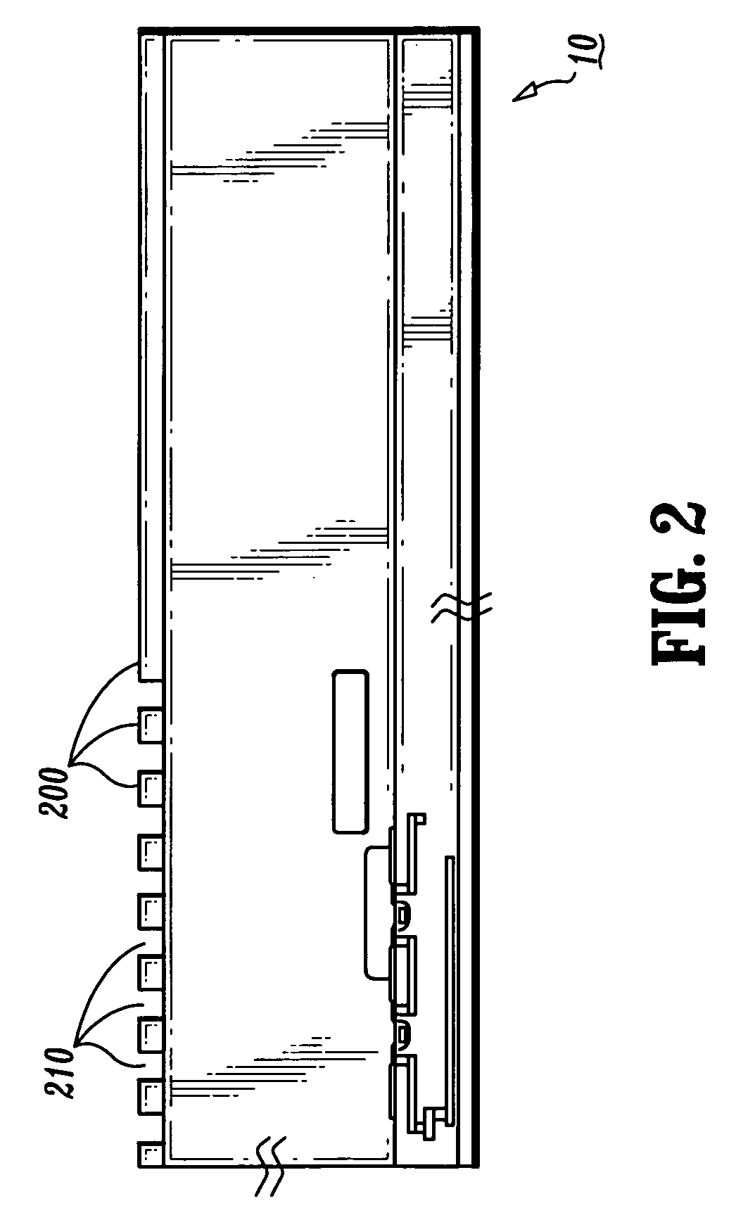
[0029]The present invention relates to the construction of thermal trenches from the backside of a wafer to improve efficiency of heat transfer from a front-side to the backside of an integrated-circuit chip. In addition, the fabrication of deep trenches from the backside of the wafer increases the depth of the trench and the number of trenches that can be constructed, and provides a means to attach heat sinks directly to the backside of the chip.

[0030]Referring now to the drawings, FIGS. 1–5 show a method of fabricating backside deep trenches on ...


PUM


Abstract

A cooling system for a semiconductor substrate incudes a plurality of trenches formed from a backside of the semiconductor substrate, and thermally conductive material deposited in the plurality of trenches. A method of forming cooling elements in a semiconductor substrate, includes coating a backside of the semiconductor substrate with a first mask layer, forming a plurality of trench patterns in the first mask layer, etching the semiconductor substrate to form a plurality of trenches along the plurality of trench patterns, and depositing thermally conductive material in the plurality of trenches. Trenches constructed from the backside of a wafer improve efficiency of heat transfer from a front-side to the backside of an integrated-circuit chip. The fabrication of trenches from the backside of the wafer allows for increases in the depth and number of trenches, and provides a means to attach passive and active cooling devices directly to the backside of a wafer.

Description

BACKGROUND OF THE INVENTION[0001]1. Field of the Invention[0002]The present invention relates to a cooling system for a semiconductor device and a method of fabricating same and, more particularly, to a cooling system including backside trenches and a method of fabricating same.[0003]2. Description of the Related Art[0004]The advent of nanotechnology has resulted in an exponential growth of integrated circuit density. The increasingly dense integrated circuits generate more thermal heat than past circuits. However, many known passive or active semiconductor cooling systems are incapable of adequately dissipating excessive amounts of thermal heat.[0005]In addition, the increase of wafer thickness due, in part, to the use of an extra oxide layer as a result of silicon-on-insulator (SOI) technology, will require more sophisticated cooling systems. In order to compensate for additional thermal resistance on the backside of the wafer, these cooling systems can be placed as close to the c...

Claims


Application Information

Patent Timeline
Patent Type & Authority Patents(United States)
IPC IPC(8): H01L21/44H01L21/20H01L23/10H01L21/48H01L23/367
CPCH01L21/4871H01L23/3677H01L23/473H01L2924/01079H01L2924/15311H01L25/0655H01L2224/16225H01L2924/01019H01L2924/10158H01L2224/05008H01L2224/05548H01L2224/05001H01L2924/00014H01L2224/05599H01L2224/05099
Inventor CHEN, HOWARD HAOHSU, LOUIS L.SHEPARD, JR., JOSEPH F.
Owner GLOBALFOUNDRIES U S INC
Why Eureka
Try Eureka