Apparatus and methods for digital-to-analog conversion

a digital-to-analog and analog conversion technology, applied in the field of digital-to-analog conversion, can solve the problems of delta-sigma modulation, inability of transmitters to transmit multiple carriers simultaneously, and inability to achieve delta-sigma modulation commercial applications such as cellular networks, so as to reduce the word length of the input signal.

Active Publication Date: 2006-04-18
NORTHROP GRUMMAN SYST CORP
View PDF2 Cites 17 Cited by
  • Summary
  • Abstract
  • Description
  • Claims
  • Application Information

AI Technical Summary

Benefits of technology

[0006]In one embodiment, the present invention is directed to an apparatus for converting a digital input signal to an analog signal for transmission, wherein the input signal can include more than one carrier signal. The apparatus includes a plurality of delta-sigma modulation loop circuits, each loop circuit having an operating frequency, wherein the loop circuits are connected in an increasing order of operating frequency so as to reduce a word length of the input signal to obtain a digital signal having a reduced word length. A tuning circuit adjusts a frequency of the digital signal to a transmitting frequency. A digital-to-analog converter converts the frequency-adjusted digital signal to an analog signal.

Problems solved by technology

It currently is not feasible for a transmitter to transmit multiple carriers simultaneously because digital-to-analog converters (DACs) currently utilized in the transmitters do not provide enough bandwidth with signal-to-noise ratios (SNRs) high enough to support multiple transmissions and still comply with FCC noise limitations.
LO sources and mixers, however, can drift in frequency with changes in temperature.
Delta-sigma modulation techniques are known in connection with signal conversion; however, delta-sigma modulation has been impractical for commercial RF applications such as cellular networks.
Fabricating such circuitry would be prohibitively expensive, however, because of the high cost, and low circuit yield of indium phosphide wafer production.
Such a CMOS-based chip, however, would require operation at clock rates which are beyond state of the art for commercial CMOS technology.

Method used


Image

  • Apparatus and methods for digital-to-analog conversion
  • Apparatus and methods for digital-to-analog conversion
  • Apparatus and methods for digital-to-analog conversion

Examples


Embodiment Construction

[0017]The following description of the preferred embodiments is merely exemplary in nature and is in no way intended to limit the invention, its application, or uses.

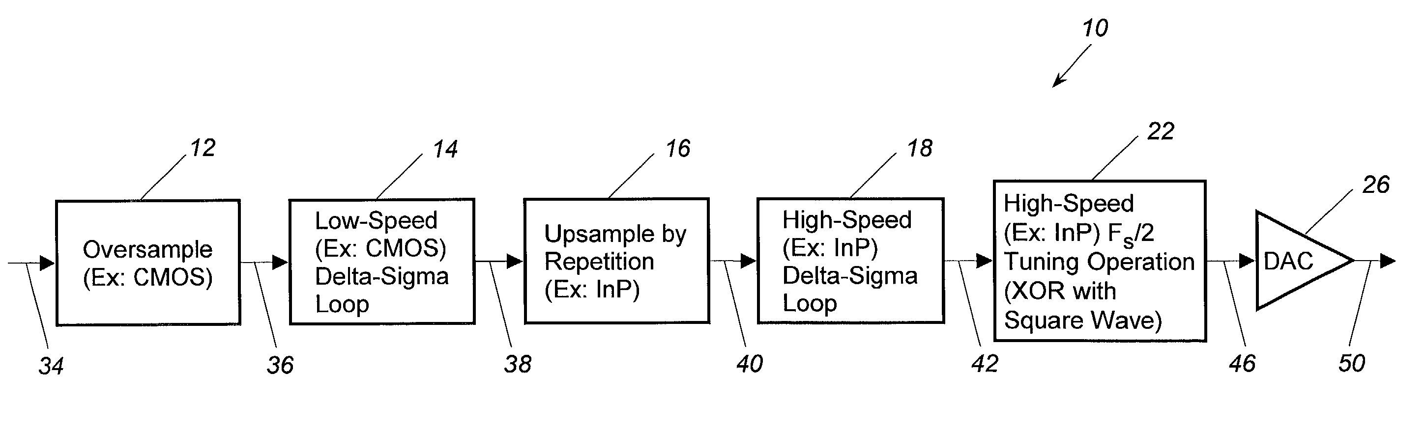
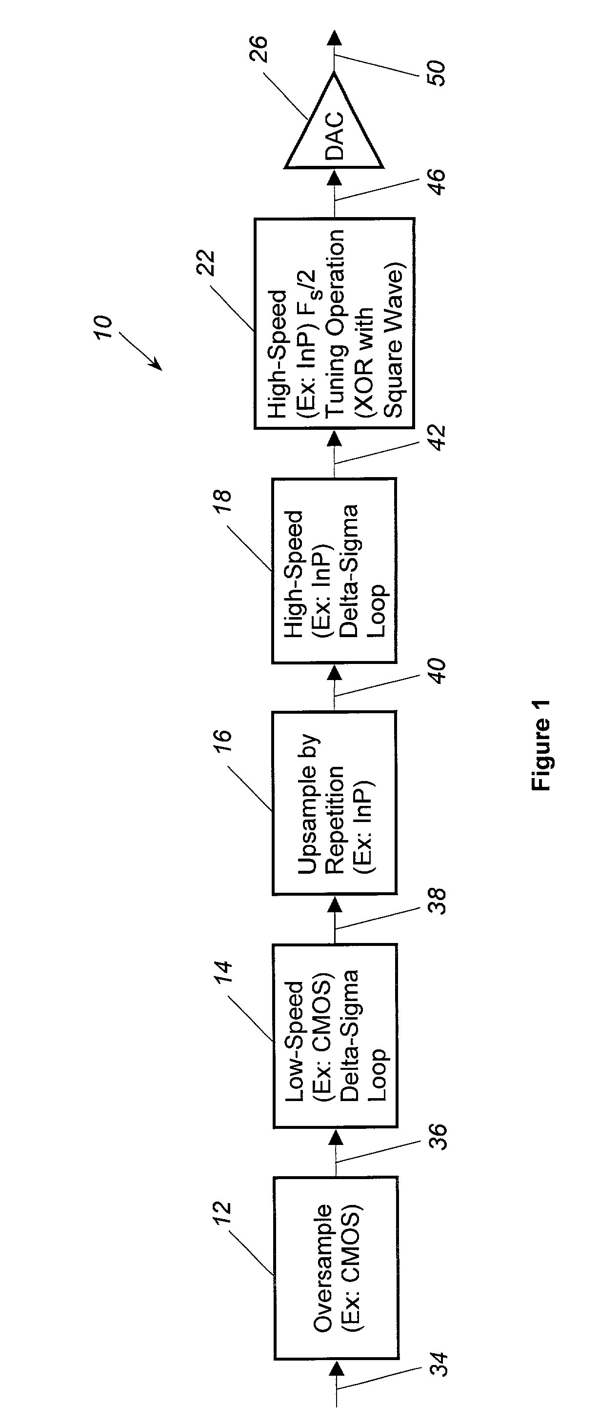
[0018]A preferred embodiment of a multiple-stage delta-sigma digital-to-analog conversion circuit is generally indicated in FIG. 1 by reference number 10. The conversion circuit or apparatus 10 includes an over-sampling circuit 12 that precedes a low-speed delta-sigma loop circuit 14. The loop circuit 14 is followed by an up-sampling circuit 16, a high-speed delta-sigma loop circuit 18, a high-speed tuning operator or circuit 22, and a one-bit digital-to-analog converter (DAC) 26. The terms “low-speed” and “high-speed” are used herein in a relative sense to refer to the frequencies of technologies respectively utilized in implementing embodiments of the invention. For example, the delta-sigma loop 14 in one embodiment is implemented using complementary metal-oxide semiconductor (CMOS) hardware, and the delta-sigma loop ...


PUM


Abstract

An apparatus for converting a digital input signal to an analog signal for transmission. The input signal can include more than one carrier signal. A plurality of delta-sigma modulation loop circuits are connected in an increasing order of operating frequency so as to reduce a word length of the input signal. A tuning circuit adjusts the signal frequency to a transmitting frequency for conversion to analog by a digital-to-analog converter. A first loop circuit is implemented using CMOS gates, and a second loop circuit and the tuning circuit are implemented using indium phosphide gates. The apparatus allows a high-resolution, wide-band RF multiple-carrier signal to be re-quantized to a lower-resolution signal while an acceptable signal-to-noise ratio is maintained.

Description

BACKGROUND OF THE INVENTION[0001]1 Field of the Invention[0002]The present invention relates generally to digital-to-analog conversion and, more particularly, to an apparatus for digital-to-analog conversion via multiple stages of delta-sigma modulation.[0003]2. Discussion of the Related Art[0004]Base stations for wireless telephone networks typically have a plurality of transmitters, each transmitter being able to transmit only one carrier at a time. It currently is not feasible for a transmitter to transmit multiple carriers simultaneously because digital-to-analog converters (DACs) currently utilized in the transmitters do not provide enough bandwidth with signal-to-noise ratios (SNRs) high enough to support multiple transmissions and still comply with FCC noise limitations. Thus current methods for converting an RF multi-carrier signal for transmission involve breaking up the RF signal band into smaller sub-bands. Each sub-band is converted to an analog signal using a digital-to...

Claims


Application Information

Patent Timeline
Patent Type & Authority Patents(United States)
IPC IPC(8): H03M3/00H04B14/06H03M3/02H04L5/02H04L27/26
CPCH04L5/023H03M7/302H04L27/2627H03M3/50H03M3/00
Inventor HINRICHS, JEFFREY M.ROSENKOETTER, BRIAN J.HARNDEN, ROBERT R.WEBER, KENNETH B.KINTIS, MARKMARTIN, DONALD R.SKONES, WILLIAM M.JOHNSON, KAI E.
Owner NORTHROP GRUMMAN SYST CORP
Why Eureka
Try Eureka