Method for polishing a substrate surface

Inactive Publication Date: 2006-05-02
RENESSELAER POLYTECHNIC INST +1
View PDF13 Cites 69 Cited by
  • Summary
  • Abstract
  • Description
  • Claims
  • Application Information

AI Technical Summary

Benefits of technology

[0010]According to another aspect of the invention, the act of preparing includes cleaning a polishing apparatus prior to polishing the surface of the substrate to substantially reduce contamination of the polishing surface. According to one aspect of the invention, the act of finishing the surface of the substrate includes an act of substantially rinsing the abrasive suspension from the surface of the substrate. According to another aspect of the invention, the method furth

Problems solved by technology

First, the slurry weakens the wafer surface and the slurry particles, in addition to particles located on the pad, complete material removal from the wafer surface.
It is desired to use aluminum nitride (AlN) as a substrate material for creating co

Method used


Image

  • Method for polishing a substrate surface
  • Method for polishing a substrate surface
  • Method for polishing a substrate surface

Examples


example

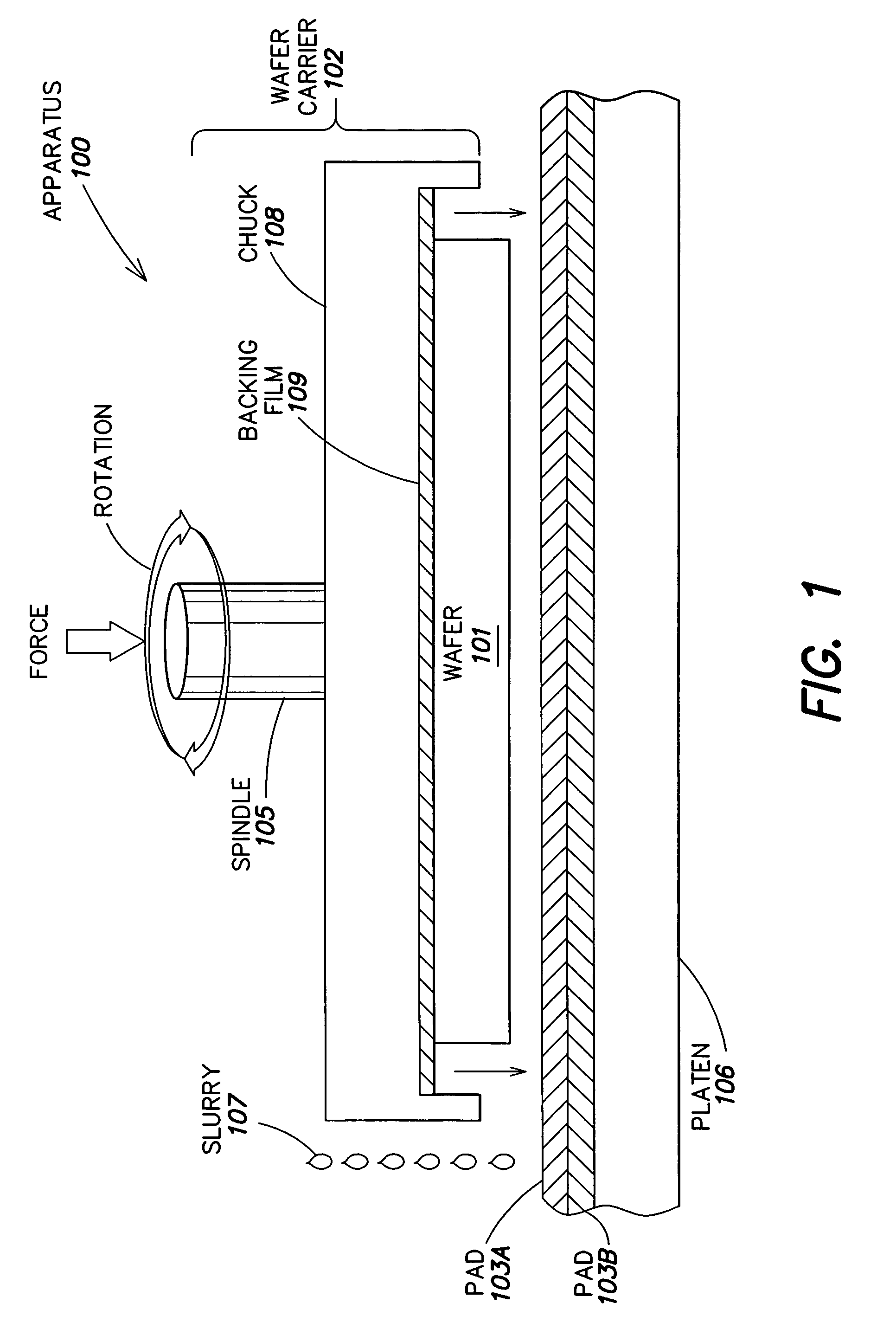
[0036]FIG. 1 shows a conventional CMP apparatus that may be used to polish substrate surfaces in a CMP process according to one embodiment of the invention. A wafer 101 to be polished is mounted on a wafer carrier 102 which generally includes a backing film 109 positioned between wafer 101 and a chuck 108 which holds the wafer and the wafer carrier 102. Wafer carrier 102 is rotated by a spindle 105. A force is applied to the wafer carrier 102 to contact the wafer 101 with one or more polishing pads 103A–103B. The one or more polishing pads 103A–103B are adhered to a platen 106 which also rotates. Further, a slurry 107 is applied to the pad 103A–103B and the drip rate is controlled, for example, by a control flow dispenser (not shown).

[0037]It should be appreciated that other CMP tools and / or polishing apparatus may be used and the invention is not limited to any particular CMP tools or polishing configurations.

[0038]According to one aspect of the invention, the CMP process may invol...


PUM


Abstract

According to one aspect of the invention, an improved process for preparing a surface of substrate is provided wherein the surface of the substrate is prepared for a chemical mechanical polishing (CMP) process, the CMP process is performed on the surface of the substrate, and the surface of the substrate is finished to clear the substrate surface of any active ingredients from the CMP process. Also, an improved substrate produced by the method is provided. According to one aspect of the invention, particular polishing materials and procedures may be used that allow for increased quality of AlN substrate surfaces.

Description

RELATED APPLICATION[0001]This application claims the benefit under Title 35, U.S.C. § 119(e) of U.S. Provisional Application Ser. No. 60 / 331,868, filed Nov. 20, 2001, entitled “Chemical Mechanical Polishing (CMP) Process” by Leo J. Schowalter, J. Carlos Rojo, Javier Martinez Lopez and Kenneth Morgan, the contents of which are incorporated herein by reference.[0002]This invention was made in part with government support under grant number F33615-98-C-1325 from the United States Air Force, Air Force Research Laboratory, and grant numbers N00014-00-M-0160 and N00014-01-C-0232 from the Department of the Navy, Office of Naval Research. The government may have certain rights in this invention.FIELD OF THE INVENTION[0003]The present invention relates generally to the preparation of semiconductor substrate surfaces, and more specifically to preparing substrate surfaces using chemical mechanical polishing (CMP).BACKGROUND OF THE INVENTION[0004]Chemical mechanical polishing (CMP) is a process...

Claims


Application Information

Patent Timeline
IPC IPC(8): H01L21/302H01L21/461B24B37/04C09G1/02H01L21/02H01L21/304H01L21/306
CPCB24B37/0056B24B37/044H01L21/02024H01L21/02052B24B49/006H01L21/30625
Inventor SCHOWALTER, LEO J.LOPEZ, JAVIER MARTINEZROJO, JUAN CARLOSMORGAN, KENNETH
Owner RENESSELAER POLYTECHNIC INST
Why Eureka
Try Eureka