Electron beam exposure apparatus and electron beam processing apparatus

an exposure apparatus and electron beam technology, applied in the field of electron beam exposure apparatus and electron beam processing apparatus, can solve the problems of complex correction data function, to be supplied to respective deflectors, and difficulty in correcting the rotation of electron beam caused by the exposure of the electron beam

Inactive Publication Date: 2006-05-09
ADVANTEST CORP +2
View PDF5 Cites 11 Cited by
  • Summary
  • Abstract
  • Description
  • Claims
  • Application Information

AI Technical Summary

Benefits of technology

[0027]The first electromagnetic lens system may reduce the plurality of electron beams that were incident on the first plane, respectively, and may make the reduced electron beams be incident on the second plane. Also, the second electromagnetic lens system may reduce the plurality of electron beams that were incident on the second plane, respectively, and may make the reduced electron beams be incident on the wafer.
[0028]Each of the first rotation correction lenses may correct rotation of a corresponding one of the electron beams that passes therethrough, based on a position on the wafer on which the corresponding electron beam is incident.
[0029]Each of the first rotation correction lenses may correct rotation of a corresponding one of the electron beams that passes therethrough, based on a position on the first plane at which the corresponding electron beam passes through the first plane.

Problems solved by technology

However, the electron beam exposure apparatus disclosed in Japanese Patent Application Laying-Open No. 11-176737 has a problem that a function for calculating correction data, that is to be supplied to respective deflectors, becomes complex since the correction data is calculated in accordance with the transferred position on the wafer, the height of the wafer, the beam current and the way in which the patterns are scattered to respective deflectors.
In addition, the electron beam exposure apparatuses disclosed in Japanese Patent Application Laid-Open Nos. 9-245708 and 2001-267221 have a problem that it is difficult to correct rotation of an image of the electron beam that is caused when the cross section of the electron beam is reduced.

Method used


Image

  • Electron beam exposure apparatus and electron beam processing apparatus
  • Electron beam exposure apparatus and electron beam processing apparatus
  • Electron beam exposure apparatus and electron beam processing apparatus

Examples


embodiment 1

(Embodiment 1)

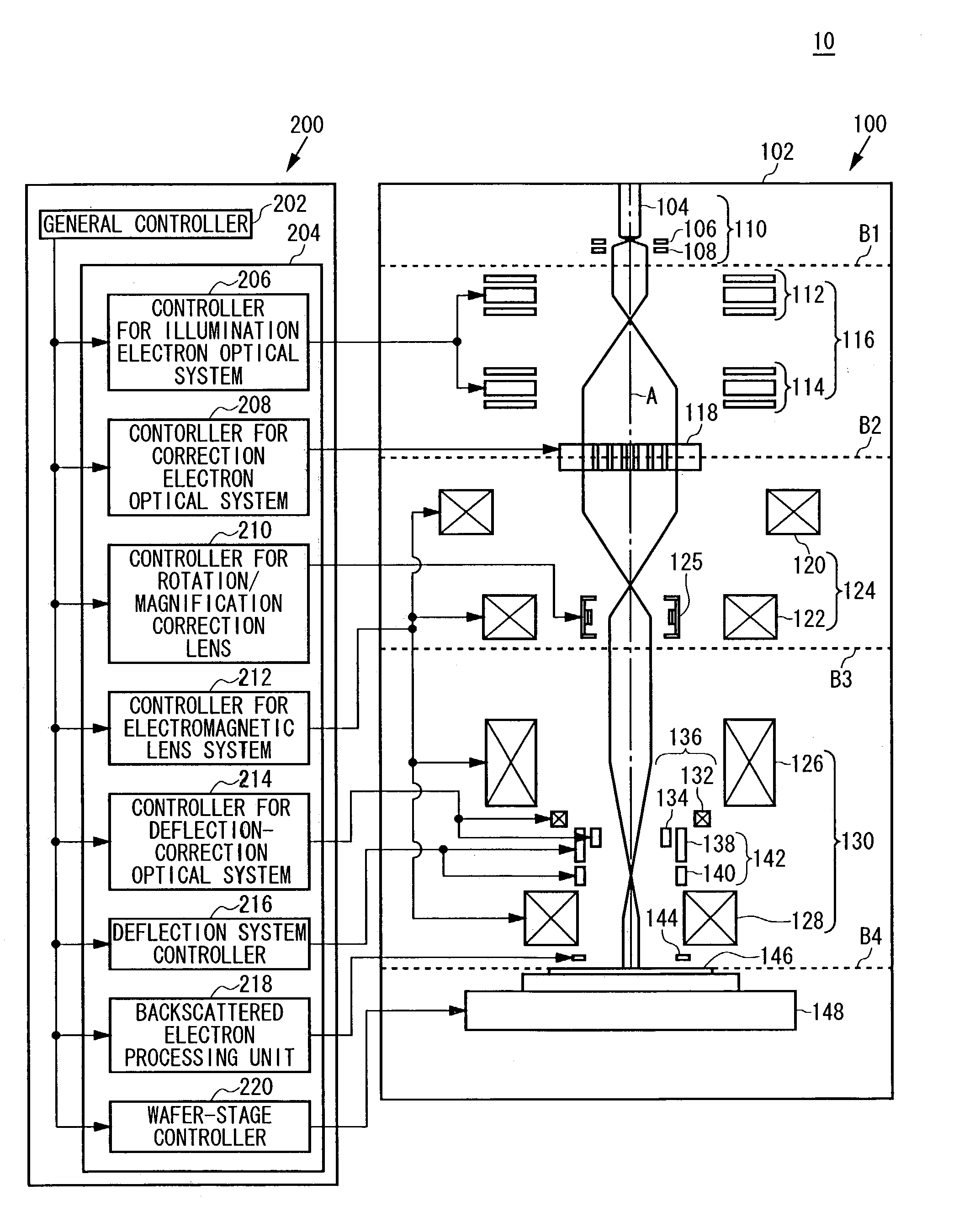
[0068]FIG. 1 illustrates an exemplary structure of an electron beam exposure apparatus 10 according to the first embodiment of the present invention. The electron beam exposure apparatus 10 includes an exposure unit 100 for performing a predetermined exposure process for wafer 146 and a controlling system 200 for controlling operations of respective units in the exposure unit 100. Please note that a dot-dashed line represents an optical axis A of an electron beam and a dotted line represents focal planes B1, B2, B3 and B4 of the electron beam.

[0069]The exposure unit 100 includes, within a body 102, an electron gun 110 that generates an electron beam to make it be incident on the focal plane B1; an illumination electron optical system 116 that enlarges the cross section of the electron beam incident on the focal plane B1 and makes the electron beam having the enlarged cross section be incident on the focal plane B2; a correction electron optical system 118 that splits t...

embodiment 2

(Embodiment 2)

[0102]FIG. 3 illustrates an exemplary structure of an electron beam exposure apparatus 1010 according to the second embodiment of the present invention. The electron beam exposure apparatus 1010 includes an exposure unit 1100 for performing a predetermined exposure process for wafer 1146 and a controlling system 1200 for controlling operations of respective units in the exposure unit 1100. Please note that a dot-dashed line represents an optical axis A of an electron beam and a dotted line represents focal planes B1, B2, B3 and B4 of the electron beam.

[0103]The exposure unit 1100 includes, within a body 1102, a plurality of electron guns 1110 that respectively generate a plurality of electron beams and make them be incident on the focal plane B1; an illumination electron optical system 1116 that enlarges the cross section of each of the electron beams incident on the focal plane B1 and converges the electron beams to make it be incident on the focal plane B2; a plurali...


PUM


Abstract

An electron beam exposure apparatus for exposing wafer with an electron beam, includes: a first electromagnetic lens system for making the electron beam incident substantially perpendicularly on a first plane be incident on a second plane substantially perpendicularly; a second electromagnetic lens system for making the electron beam that was substantially perpendicularly incident on the second plane be incident on the wafer substantially perpendicularly; a rotation correction lens provided within the first electromagnetic lens system for correcting rotation of the electron beam caused by at least the first electromagnetic lens system; a deflection system for deflecting the electron beam to a position on the wafer; and a deflection-correction optical system provided within the second electromagnetic lens system for correcting deflection aberration caused by the deflection system.

Description

[0001]This patent application claims priority from Japanese patent applications Nos. 2002-135891 and 2002-135892 both filed on May 10, 2002, the contents of which are incorporated herein by reference.BACKGROUND OF THE INVENTION[0002]1. Field of the Invention[0003]The present invention relates to an electron beam exposure apparatus and an electron beam processing apparatus. More particularly, the present invention relates to an electron beam exposure apparatus which can expose wafer with using an electron beam or a plurality of electron beams so that a pattern is transferred onto the wafer with high precision.[0004]2. Description of the Related Art[0005]With the size reduction of semiconductor devices in recent years, various electron beam exposure apparatuses have been developed in order to improve the resolution and throughput of the semiconductor devices. For example, Japanese Patent Application Laying-Open No. 11-176737 discloses an electron beam apparatus that corrects deflectio...

Claims


Application Information

Patent Timeline
Patent Type & Authority Patents(United States)
IPC IPC(8): G21G5/00G21K5/10G21K1/093H01J37/153H01J37/317
CPCB82Y10/00B82Y40/00H01J37/153H01J37/3177G21K1/093H01J2237/1536
Inventor HAMAGUCHI, SHINICHIGOTO, SUSUMUKAMIMURA, OSAMUSOHDA, YASUNARI
Owner ADVANTEST CORP
Why Eureka
Try Eureka