Non-volatile memory cell having a silicon-oxide nitride-oxide-silicon gate structure

a silicon-oxide, non-volatile technology, applied in the direction of solid-state devices, semiconductor devices, instruments, etc., can solve the problems of affecting the erase operation, the threshold voltage of the memory cell b>5/b> cannot be completely erased, and the memory device cannot reach the necessary prescribed condition

Inactive Publication Date: 2006-05-09
SAMSUNG ELECTRONICS CO LTD
View PDF21 Cites 41 Cited by
  • Summary
  • Abstract
  • Description
  • Claims
  • Application Information

AI Technical Summary

Problems solved by technology

Volatile memory devices lose their stored data when their power supplies are interrupted, while nonvolatile memory devices retain their stored data even when their power supplies are interrupted.
However, when an excessive amount of electrons are trapped in the trapping region 7 of the charge trapping layer 12, or not enough holes can be injected into the trapping region to bring the memory cell to its former condition, then the threshold voltage of the memory cell 5 cannot be completely erased, i.e., cannot reach the necessary prescribed condition.
The fact that electrons are trapped in an area far away from the highly doped area 17 (functioning as the drain or source) may adversely affect the erase operation.

Method used


Image

  • Non-volatile memory cell having a silicon-oxide nitride-oxide-silicon gate structure
  • Non-volatile memory cell having a silicon-oxide nitride-oxide-silicon gate structure
  • Non-volatile memory cell having a silicon-oxide nitride-oxide-silicon gate structure

Examples


Embodiment Construction

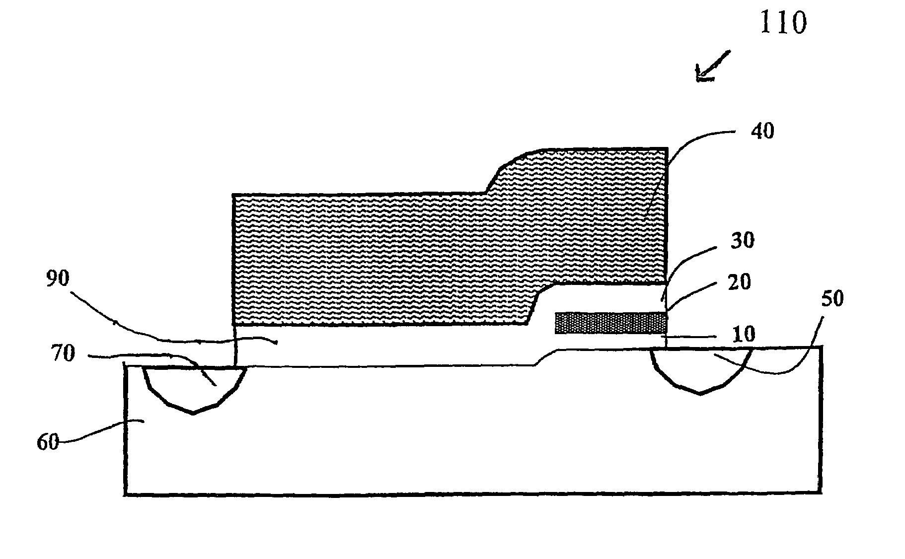
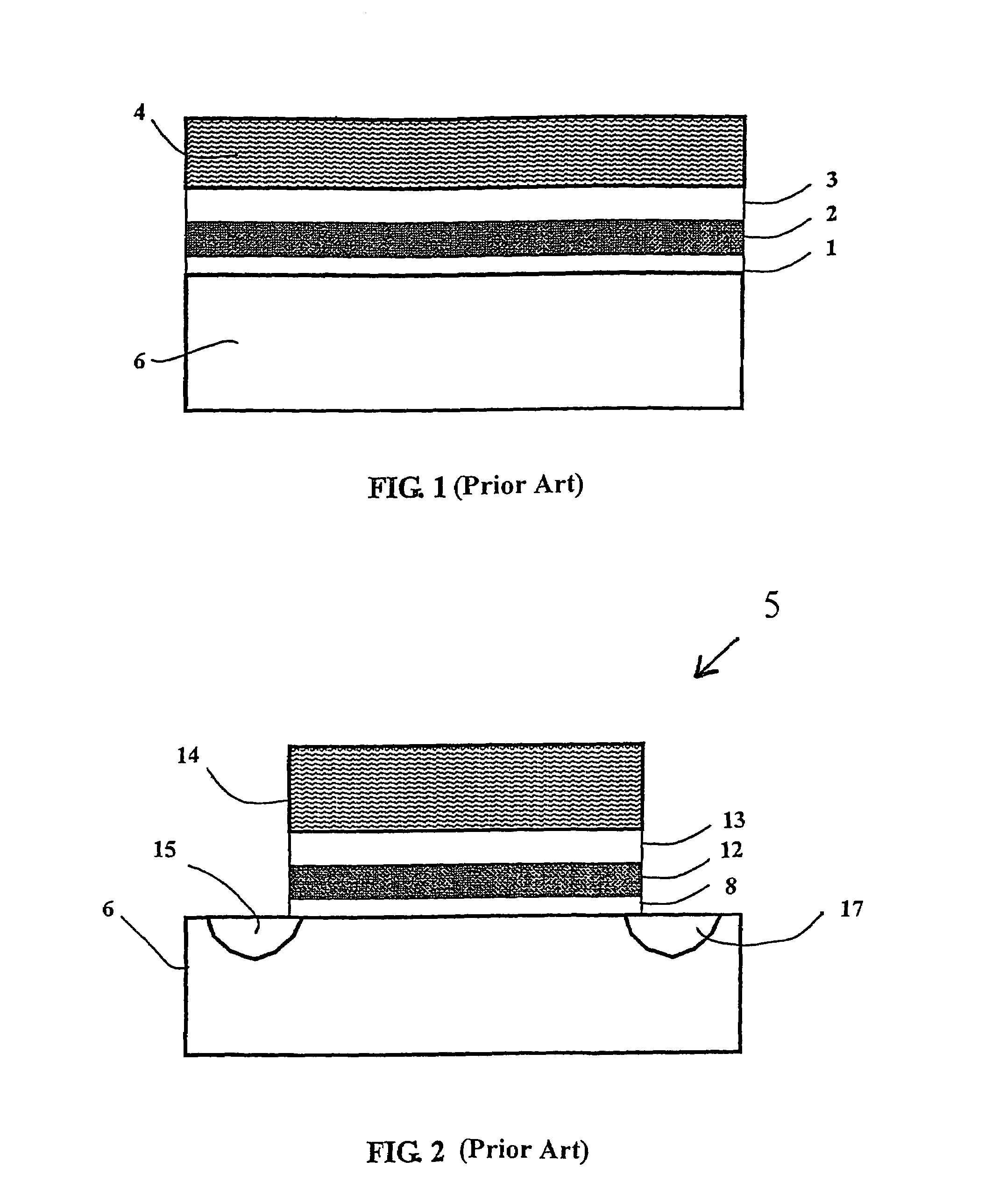
[0030]FIG. 5 is a cross-sectional view of a non-volatile memory cell 110 having a SONOS structure, according to embodiments of the invention. The memory cell 110 includes, formed on a substrate 60, a tunneling layer 10, a charge trapping layer 20, a blocking layer 30, and a control gate electrode 40. Additionally formed on the substrate 60 is a gate insulating layer 90. Formed within the substrate 60, substantially below edges of the control gate 40 are a drain 50 and a source 70, which are made by doping the substrate appropriately. The functions of the drain 50 and source 70 can be interchanged by applying a biasing voltage, as discussed below. As shown in FIG. 5, the charge trapping layer 20 does not extend fully across the length of the memory cell 110, but only across a portion thereof. Additionally, as shown in FIG. 6, the memory cell 110 can also include a metal silicide layer 100 formed on the control gate 40. The metal in the metal silicide layer 100 could be, for example, ...


PUM


Abstract

A non-volatile memory cell able to be written in a first direction and read in a second direction is described. The memory cell includes one or two charge trapping regions located near either the source or the drain, or both the source and the drain. During a programming operation, electrons can be injected into the charge trapping region by hot electron injection. During an erasing operation, holes can be injected into the charge trapping region. Embodiments of the invention include a charge trapping region that is overlapped by the control gate only to an extent where the electrons that were injected during a programming operation can be erased later by injecting holes in the charge trapping region.

Description

TECHNICAL FIELD[0001]This disclosure relates to non-volatile memory cells, and, more particularly, to memory cells having Silicon-Oxide-Nitride-Oxide-Silicon gate structures.BACKGROUND OF THE INVENTION[0002]Semiconductor memory devices that are used for storing data can generally be categorized as being either volatile or non-volatile memory devices. Volatile memory devices lose their stored data when their power supplies are interrupted, while nonvolatile memory devices retain their stored data even when their power supplies are interrupted. Thus, nonvolatile memory devices are widely used in situations where power is not always available, is frequently interrupted, or when low power usage is required, such as in mobile telecommunication systems, memory cards for storing music and / or image data, and in other applications.[0003]Generally, cell transistors in non-volatile memory devices have a stacked gate structure. The stacked gate structure includes, sequentially stacked on a chan...

Claims


Application Information

Patent Timeline
Patent Type & Authority Patents(United States)
IPC IPC(8): H01L29/788H01L21/8247G11C16/04H01L21/28H01L21/336H01L21/8238H01L21/8239H01L27/105H01L27/115H01L29/51H01L29/792
CPCH01L21/28185H01L29/792H01L29/4234H01L29/513H01L29/518H01L29/66833H01L21/28282G11C16/0466H01L21/28194H01L21/28202H01L21/28211H01L29/40117H10B99/00
Inventor KANG, SUNG-TAEGKIM, SEUNG-GYUNHAN, JUNG-WOOKYOO, HYUN-KHE
Owner SAMSUNG ELECTRONICS CO LTD
Why Eureka
Try Eureka