Semiconductor package

a technology of semiconductors and encapsulants, applied in the direction of semiconductor/solid-state device details, semiconductor devices, electrical apparatus, etc., can solve the problems of chip b>12/b> in the encapsulant b>20/b> warpage or stress, package b>10/b> to warpage or stress, etc., to reduce the thermal stress of the package and reduce the stress of the chip

Active Publication Date: 2006-05-09
ADVANCED SEMICON ENG INC
View PDF2 Cites 0 Cited by
  • Summary
  • Abstract
  • Description
  • Claims
  • Application Information

AI Technical Summary

Benefits of technology

[0009]It is an object of the present invention to provide a low stress semiconductor package which has a chip disposed on and spaced apart from a substrate or a carrier so as to reduce the stress of the chip.
[0010]In order to achieve the above object, the present invention provides a semiconductor package comprising spacers, a chip, bonding wires, contacts, a substrate, and an encapsulant. The spacers are disposed on the substrate, and the chip is disposed on the spacers. The bonding wires are electrically connected to the chip and the contacts. The contacts are electrically connected to an external circuit board. The encapsulant encapsulates the spacers and the active and back surfaces of the chip and, therefore, the thermal stress of the package is reduced.
[0011]In the semiconductor package according to the present invention, the adhesive layer between the chip and substrate is replaced with the spacers and the encapsulant such that the chip is substantially surrounded with the encapuslant, and thus the effect of the mismatch of the coefficients of thermal expansion can be substantially reduced and the thermal stress on the chip can be substantially reduced. Further, a space is formed between the chip and substrate by the spacers and is filled with the encapsulant such that the thermal stress in the semiconductor package is modifiable by the modification of the size of the spacers or the space.

Problems solved by technology

However, the mismatch of the coefficients of thermal expansion (CTE) of the components in the package 10 leads the package 10 to warpage or stress.
In addition, the mismatch of the coefficients of thermal expansion (CTE) further leads the chip 12 in the encapsulant 20 to damage.

Method used


Image

  • Semiconductor package
  • Semiconductor package
  • Semiconductor package

Examples


Embodiment Construction

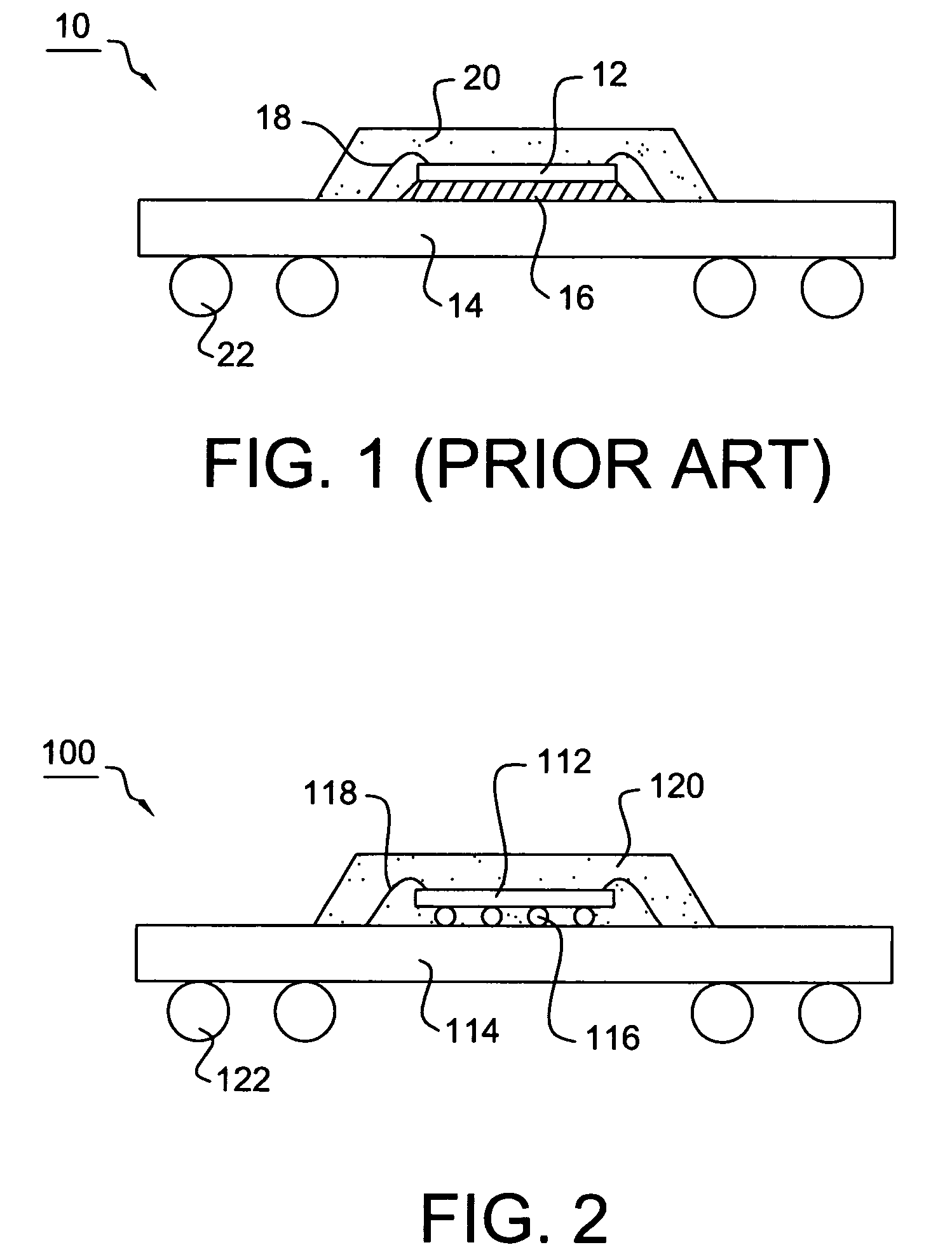
[0027]Now referring to FIG. 2, it depicts a semiconductor package 100 according to an embodiment of the present invention. The semiconductor package 100 is a ball grid array package and has a carrier, such as a circuit board or substrate 114, and a chip 112. A plurality of spacers 116 are disposed on the substrate 114, and then the chip 112 is disposed on the spacers 116 and electrically connected to the substrate 114 by bonding wires 118. An encapsulant 120 encapsulates the chip 112, the spacers 116, and the bonding wires 118. A plurality of contacts, such as solder balls 122, are electrically connected to the bonding wires 118 and disposed on the bottom surface of the substrate 114 for being attached to an external circuit of an external circuit board.

[0028]The spacers 116 can be made of polymer or glass. The spaces 116 are not limited to be spherical as shown in the drawings, and can be other shapes, such as cylindrical and cubic. The thickness of the encapsulant 120 is about 32 ...


PUM


Abstract

A semiconductor package includes spacers, a chip, bonding wires, contacts, and an encapsulant. The chip is disposed on the spacers. The bonding wires are electrically connected to the chip, and the contacts are electrically connected to the bonding wires. The contacts are electrically connected to an external circuit board. The encapsulant encapsulates the spacers and the active and back surfaces of the chip so as to lower the thermal stress of the chip.

Description

CROSS REFERENCE TO RELATED APPLICATION[0001]This application claims the priority benefit of Taiwan patent application serial No. 092110060, filed on Apr. 25, 2003, and the full disclosure thereof is incorporated herein by reference.BACKGROUND OF THE INVENTION[0002]1. Field of the Invention[0003]The present invention relates to a semiconductor package, and more particularly, to a low thermal stress semiconductor package which has a chip disposed on and spaced from a substrate.[0004]2. Description of the Related Art[0005]The semiconductor package has four major functions, i.e. signal distribution, power distribution, heat dissipation, and protection. In general, the semiconductor chip is formed into an enclosure, such as a single-chip module (SCM) or a chip carrier, referred to as the packaging of the semiconductor. These packaged chips, along with other components such as capacitors, resistors, inductors, filters, switches, and optical and RF components, are assembled to a printed wi...

Claims


Application Information

Patent Timeline
Patent Type & Authority Patents(United States)
IPC IPC(8): H01L23/52H01L23/31H01L23/495H01L25/065
CPCH01L23/3107H01L23/49575H01L24/73H01L25/0657H01L23/3128H01L25/0652H01L24/32H01L2224/16225H01L2224/32145H01L2224/32225H01L2224/48091H01L2224/48227H01L2224/48247H01L2224/73265H01L2924/01047H01L2924/01082H01L2924/15153H01L2924/15165H01L2924/15311H01L2924/1532H01L2924/19041H01L2224/83138H01L2924/1815H01L2225/06568H01L2225/06565H01L2225/06575H01L2225/06517H01L2225/0651H01L2924/01033H01L24/48H01L2924/00014H01L2924/00H01L2224/05599H01L2224/16245H01L2224/17181H01L2224/45099H01L2224/73207H01L2224/73257H01L2224/85399H01L2924/181H01L2924/351H01L2924/00012H01L2224/45015H01L2924/207
Inventor WU, JENG DA
Owner ADVANCED SEMICON ENG INC
Why Eureka
Try Eureka