Bonding pad for a packaged integrated circuit

a technology of integrated circuits and bonding pads, which is applied in the direction of printed circuit manufacturing, electrical apparatus construction details, conductive pattern formation, etc., can solve the problems of wire shorting with other wires, difficult to reliably connect wires to bonding pads, and the integration circuit is continuing to become smaller and more complex

Inactive Publication Date: 2006-05-09
TAIWAN SEMICON MFG CO LTD
View PDF43 Cites 35 Cited by
  • Summary
  • Abstract
  • Description
  • Claims
  • Application Information

AI Technical Summary

Problems solved by technology

Integrated circuits are continuing to become smaller and more complex.
Thus, it can be difficult to reliably connect the wires to the bonding pads.
Common problems are wires shorting with other wires and wires not staying attached or making good electrical contact with a bonding pad.

Method used


Image

  • Bonding pad for a packaged integrated circuit
  • Bonding pad for a packaged integrated circuit
  • Bonding pad for a packaged integrated circuit

Examples


first embodiment

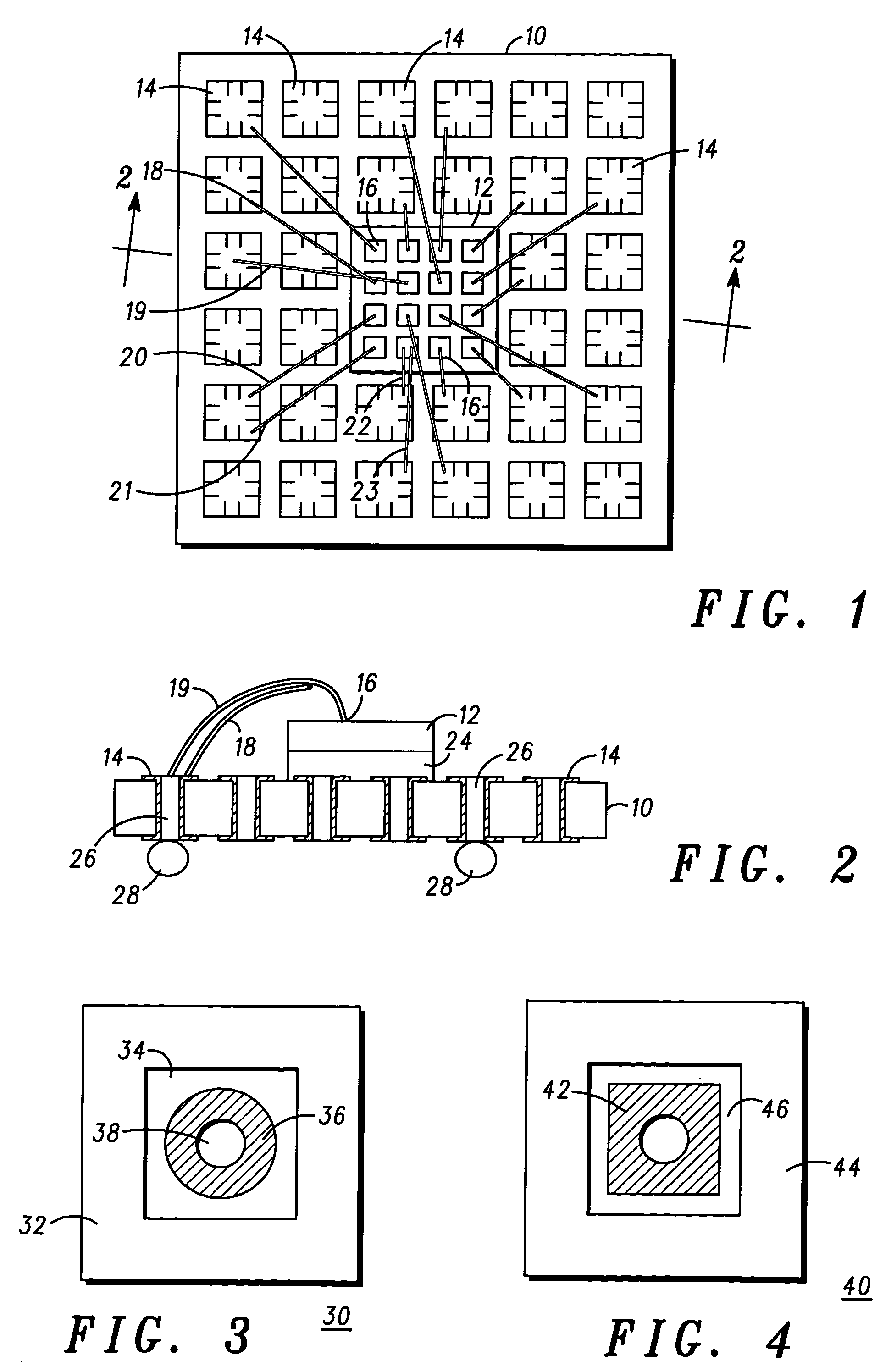
[0022]Referring now to FIGS. 3–6, various embodiments of bonding pads or via capture pads are shown. FIG. 3 is a greatly enlarged top view of a bonding pad or via capture pad 30 located on a surface of a package substrate. The bonding pad 30 is located over and in contact with a via, such as the vias 26 shown in FIG. 2. The bonding pad 30 includes a photo mask area 32. The photo mask area 32 comprises a solder mask over BT. The photo mask area 32 is preferably rectangular shaped. A clearance area 34 is located within the photo mask area 32. The clearance area 34 is an area between the bond area and the solder mask opening or a clearance of a wire loop to a land area 36. The clearance area 34 is preferably formed of the same material as the package substrate. In the presently preferred embodiment, the clearance area is formed of BT (Bismaleimide / Triazine). Further, the clearance area 34 preferably has the same shape as the photo mask area 32, e.g., rectangular shaped, although this i...

second embodiment

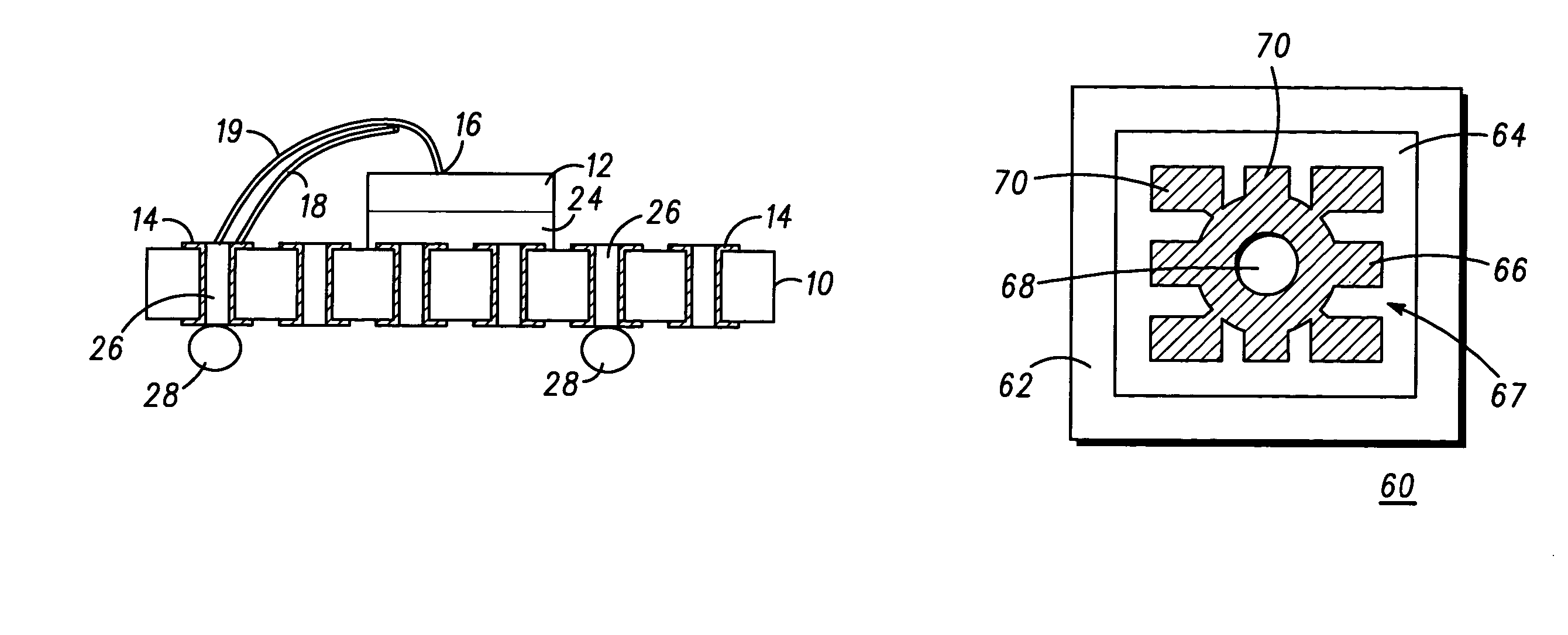
[0025]FIG. 4 shows a bonding pad 40 having the same construction as the bonding pad 30 (FIG. 3) except that it has a land area 42 that is generally rectangular. Thus, in this second embodiment, a photomask area 44, a clearance area 46 and the land area 42 all have a plurality of sharp edges that assist the pattern recognition system of the wire bonder in locating the land area 42 and attaching at least one bond wire thereto.

third embodiment

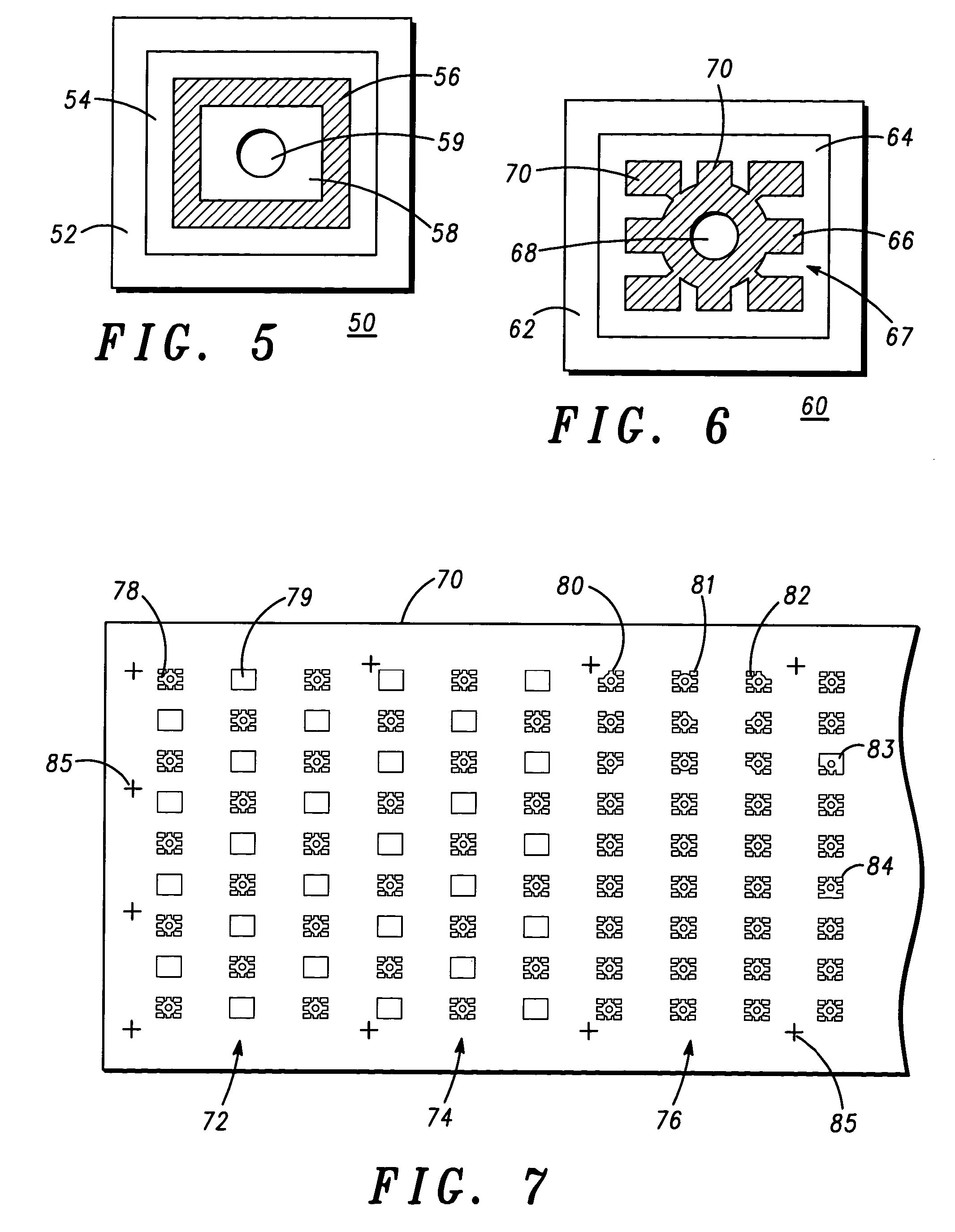
[0026]FIG. 5 is a top plan view of a bonding pad 50 in accordance with the present invention. The bonding pad 50 includes a photo mask area 52, a clearance area 54 and a land area 56 like the bonding pads 30 and 40. However, the bonding pad 50 also includes a solder mask area 58 located within the land area 56 and surrounding a via plug 59. The purpose of the solder mask area 58 is to provide sufficient clearance to ensure the via is always covered by the solder mask.


PUM

PropertyMeasurementUnit
diameteraaaaaaaaaa
diameteraaaaaaaaaa
clearance areaaaaaaaaaaa

Abstract

An integrated circuit is packaged using a package substrate that has a bottom side with a regular array of connection points and a top side with the integrated circuit on it. Vias in the package substrate provide electrical connection between the top and bottom sides. The vias have a via capture pad to which a wire may be wire bonded so that the wires from the IC to the substrate top side directly contact the vias at their capture pads without the need for traces from a top side bond pad to a via. The via capture pad is shaped to include at least one sharp edge to improve the ability of a wirebonder with pattern recognition software to locate the capture pad and place the wire.

Description

BACKGROUND OF THE INVENTION[0001]The present invention relates to packaged integrated circuits, and more particularly, to bonding pads of integrated circuits that are packaged and have wire bonds.[0002]Integrated circuits are continuing to become smaller and more complex. As circuit complexity has increased, so has the need for more input and output signals. Ball grid array (BGA) is an important package type for integrated circuits that typically uses wire bonds in making electrical connection between the integrated circuit and one part of the BGA package. BGA packages generally have an integrated circuit mounted on a top side of a package substrate and an array of solder balls on a bottom side of the package substrate. Then, bonding pads on the integrated circuit are connected to wire bond fingers on the package substrate with wires. The wire bond fingers typically are connected to traces, which in turn are connected to via capture pads to vias and finally to the solder balls on th...

Claims


Application Information

Patent Timeline
Patent Type & Authority Patents(United States)
IPC IPC(8): H01L23/02H01L23/48H01L23/52H01L23/31H01L23/498H01L23/50H01L23/544
CPCH01L23/50H01L24/49H01L23/49838H01L24/85H01L24/78H01L23/3128H01L2224/32225H01L23/544H01L24/45H01L2224/45124H01L2224/45139H01L2224/45144H01L2224/45147H01L2224/45164H01L2224/48091H01L2224/48235H01L2224/4917H01L2224/49171H01L2924/01013H01L2924/01029H01L2924/01046H01L2924/01047H01L2924/01079H01L2924/01082H01L2924/14H01L2924/15311H01L2224/85H01L2224/78H01L2924/014H01L2924/01033Y10T29/49155H01L2224/73265H01L2224/48227H01L24/48H01L2924/00014H01L2924/00H01L2924/00012H01L24/73H01L2224/05554H01L2224/45015H01L2924/12042H01L2924/20752
Inventor HARUN, FUAIDAKOH, LIANG JENTAN, LAN CHU
Owner TAIWAN SEMICON MFG CO LTD
Why Eureka
Try Eureka