Semiconductor test system having a tester and a prober and test method thereof

a test system and prober technology, applied in the direction of oscillation comparator circuits, instruments, measurement devices, etc., can solve the problems of easy ic classification, erroneous connection of interface connection, and incorrect test results obtained without self-awareness, so as to avoid incorrect test results

Inactive Publication Date: 2006-05-09
WINBOND ELECTRONICS CORP
View PDF2 Cites 5 Cited by
  • Summary
  • Abstract
  • Description
  • Claims
  • Application Information

AI Technical Summary

Benefits of technology

[0006]The primary object of the present invention is to provide a semiconductor test system having a tester and a prober and the test method thereof to avoid incorrect test results caused by erroneous connection of the test interface due to man-made carelessness.
[0007]Another object of the present invention is to provide a semiconductor test system and the test method thereof, wherein a discrimination step is performed before performing wafer test to determine whether the connection of the interface connection is correct. When the connection is incorrect, a start signal will be interrupted to disable the test system, hence accomplishing the effect of prevention.
[0010]To achieve the above objects, the present invention provides a semiconductor test system having a tester and a prober. The test system performs test with discrimination and protection functions to ensure the correctness of test results. A test mark signal and a control board having a discrimination circuit and a protection circuit are added to a test connection interface of the tester. When performing multi-chip test, the connection result is displayed after checking the test mark signal by the discrimination circuit. Whether the test can be performed or not is then determined by the protection circuit. When the interface connection is incorrect, an alarm will buzz for warning, and the protection circuit will be simultaneously activated to disable the tester. Normal test can be performed only if the interface connection is correct. Thereby, the correctness of the test results can be ensured to reduce returned purchase and to enhance the quality of production.

Problems solved by technology

As shown in FIG. 1, because wafers are tested by a semiconductor test system having no discrimination and protection functions, erroneous classification of IC may easily occur.
Moreover, when performing multi-chip test, erroneous connection of the interface connection may occur due to man-made carelessness.
If test is performed without immediately finding the error, incorrect test results will be obtained without self-awareness.
If bad products are shipped to customers, not only will they be returned, but the business credit will also be badly affected.
Therefore, erroneous classification of IC may easily arise.

Method used


Image

  • Semiconductor test system having a tester and a prober and test method thereof
  • Semiconductor test system having a tester and a prober and test method thereof
  • Semiconductor test system having a tester and a prober and test method thereof

Examples


Embodiment Construction

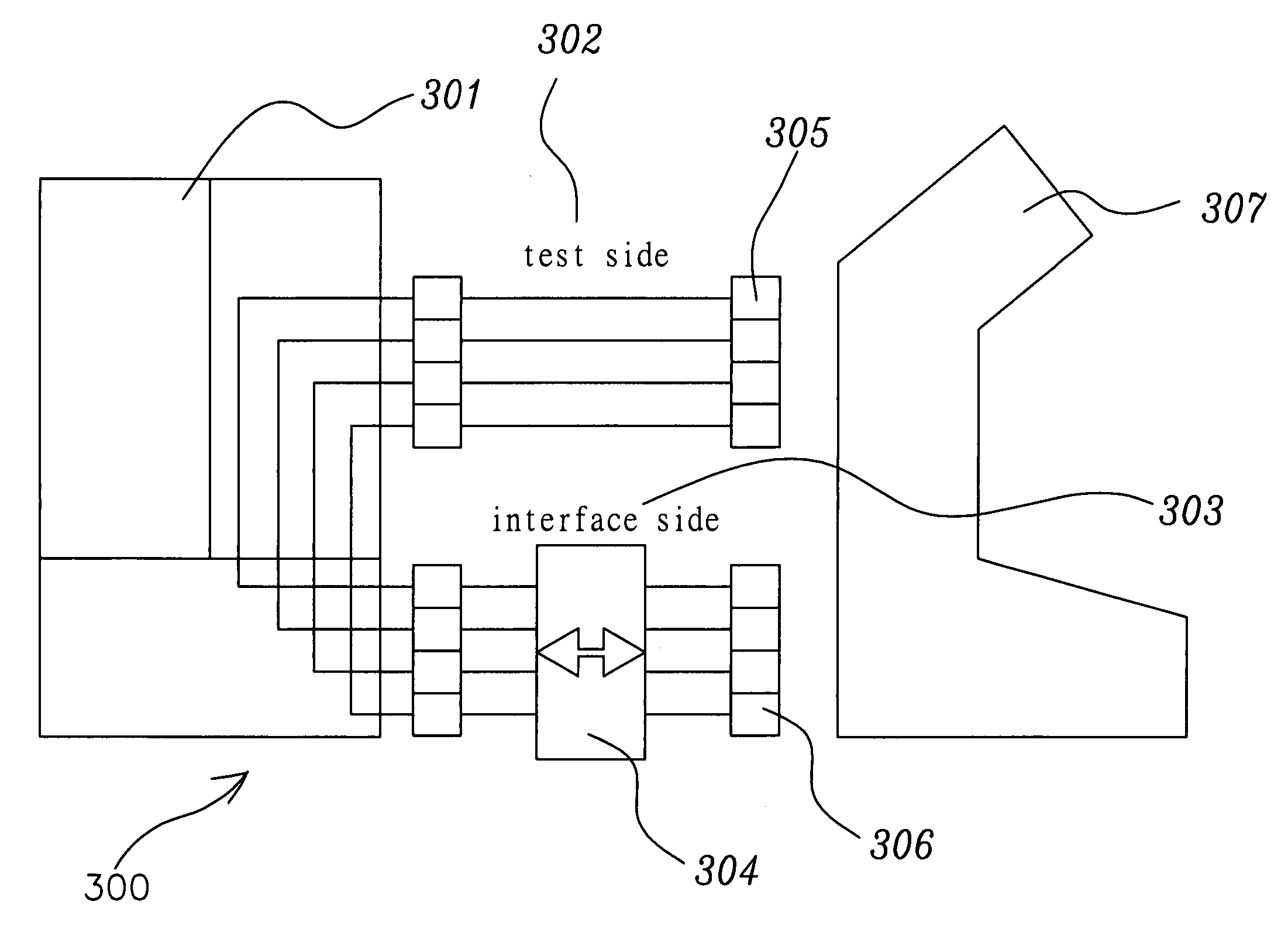
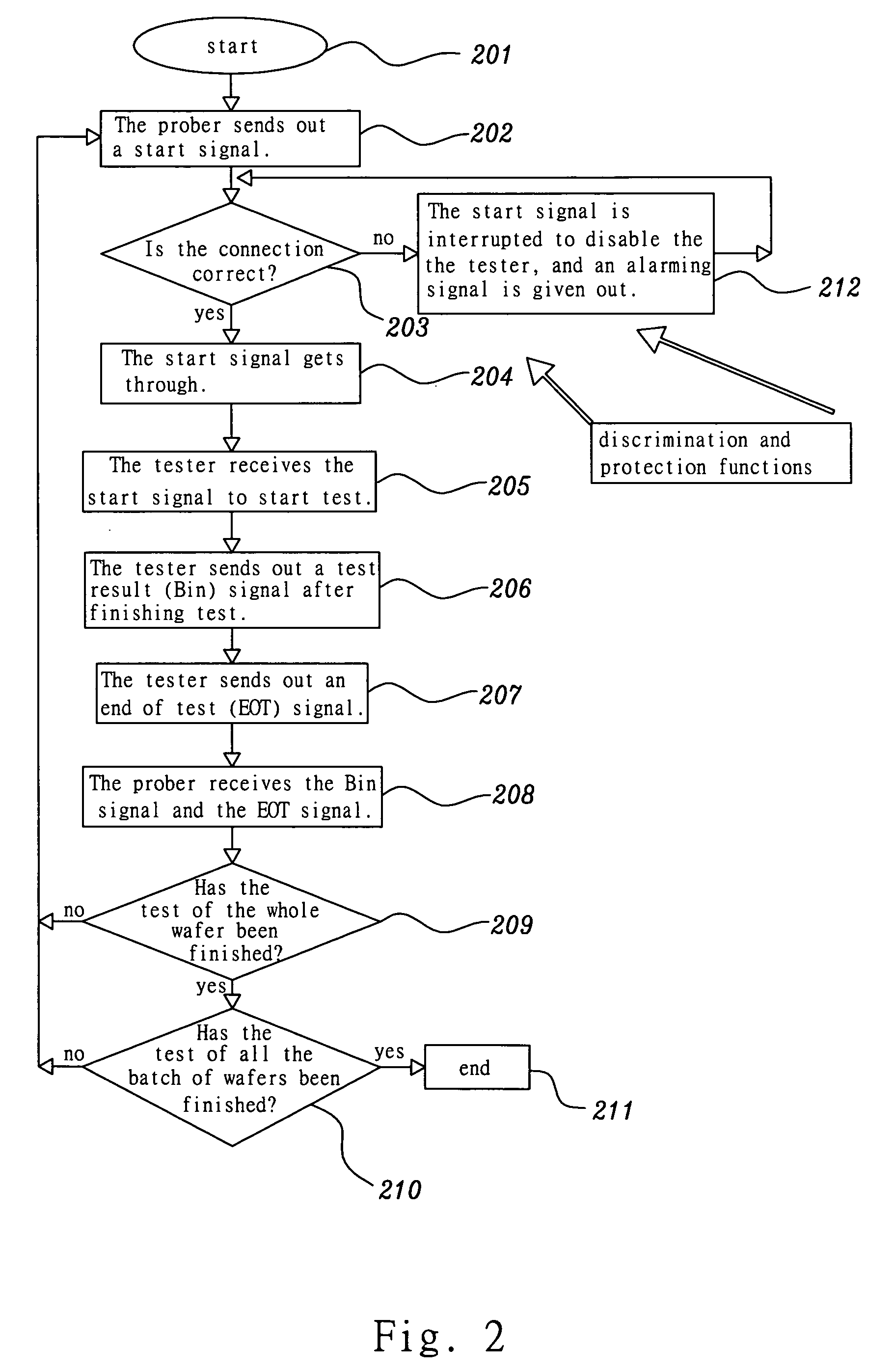
[0018]As shown in FIG. 2, a finished wafer is first prepared to be sent to a semiconductor test machine before test (Step 201). The test machine comprises a prober and a tester. When the prober successfully detects the position of a measurement point, it will immediately send out a start signal (Step 202). Meanwhile, a test mark signal and a control board having a discrimination circuit and a protection circuit are added to a test interface of the tester. The discrimination circuit is utilized to compare the test mark signal to determine whether the connection is correct (Step 203). If the connection is correct, the tester start signal gets through, and a lamp is on (Step 204). Otherwise, the tester start signal is interrupted, and the protection circuit is simultaneously activated to disable the tester (Step 212). An alarming signal is also activated to drive an alarm to buzz so as to warn the test workers. After the test workers solve the problem, Step 203 is performed again. In o...


PUM


Abstract

A semiconductor test system having a tester and a prober and the test method thereof are proposed. A test mark signal and a control board having a discrimination circuit and a protection circuit are added to a test connection interface of the tester. When performing multi-chip test, the connection result is displayed after checking the test mark signal by the discrimination circuit. Whether the test can be performed or not is then determined by the protection circuit. When the interface connection is incorrect due to man-made carelessness, an alarm will buzz for warning, and the protection circuit will be simultaneously activated to disable the tester. Normal test can be performed only if the interface connection is correct. Thereby, the correctness of the test results can be ensured to reduce returned purchase and to enhance the quality of production.

Description

[0001]The present invention relates to a semiconductor test system having a tester and a prober and the test method thereof and, more particularly, to a semiconductor test system having a tester and a prober and the test method thereof, which have discrimination and protection functions to prevent users from still performing production test without finding erroneous connection of the test interface due to man-made carelessness.BACKGROUND OF THE INVENTION[0002]In the current IC fabrication process, semiconductor testing plays an important role. After complicated semiconductor fabrication procedures of a batch of wafers have been finished, they are sent to the testing stage. Meanwhile, it is necessary to perform test of each die to discriminate quality of dies on each wafer. After packaging of normal dies is finished, commercial products in the market are obtained. Through the steps of electric or physical test of semiconductor, dies not up to the specification are immediately discard...

Claims


Application Information

Patent Timeline
Patent Type & Authority Patents(United States)
IPC IPC(8): G01R31/02
CPCG01R31/2889G01R31/045G01R31/69
Inventor HSIAO, LI-SHENG
Owner WINBOND ELECTRONICS CORP
Why Eureka
Try Eureka