Integrating tool, module, and fab level control

a technology of fab level control and tooling, applied in the field of semiconductor wafer fabrication factories, can solve the problems of fabs that require an extraordinary amount of coordination, add to the complexity of the system, and require a large amount of coordination

Inactive Publication Date: 2006-05-16
APPLIED MATERIALS INC
View PDF413 Cites 45 Cited by
  • Summary
  • Abstract
  • Description
  • Claims
  • Application Information

AI Technical Summary

Benefits of technology

[0011]The present invention addresses the problems described above by processing semiconductor wafers in a fab in a manner that integrates control at multiple functional unit levels. Examples of these levels of functional units could include fabs, modules, tools, and the like. To facilitate one or more embodiments of the present invention (as envisioned by one or more embodiments thereof), one or more first functional unit property targets (for producing a given semiconductor device or portion thereof) are initially received at a functional unit. The functional unit property targets are utilized to generate a number of other functional unit property targets. For example, it may generate a number of tool targets for any number of tool level functional units. From there, the tool targ...

Problems solved by technology

Present-day semiconductor wafer fabrication factories (or ‘fabs’) are extremely complex environments that require an extraordinary amount of coordination.
These levels of management or control, while helpful in increasing efficiency, add to the complexity of the system.
Thus, ev...

Method used


Image

  • Integrating tool, module, and fab level control
  • Integrating tool, module, and fab level control
  • Integrating tool, module, and fab level control

Examples


Embodiment Construction

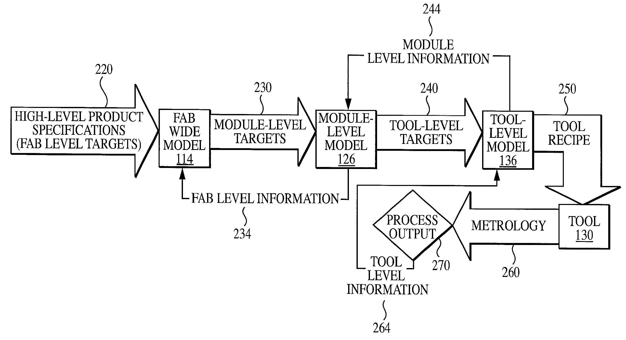
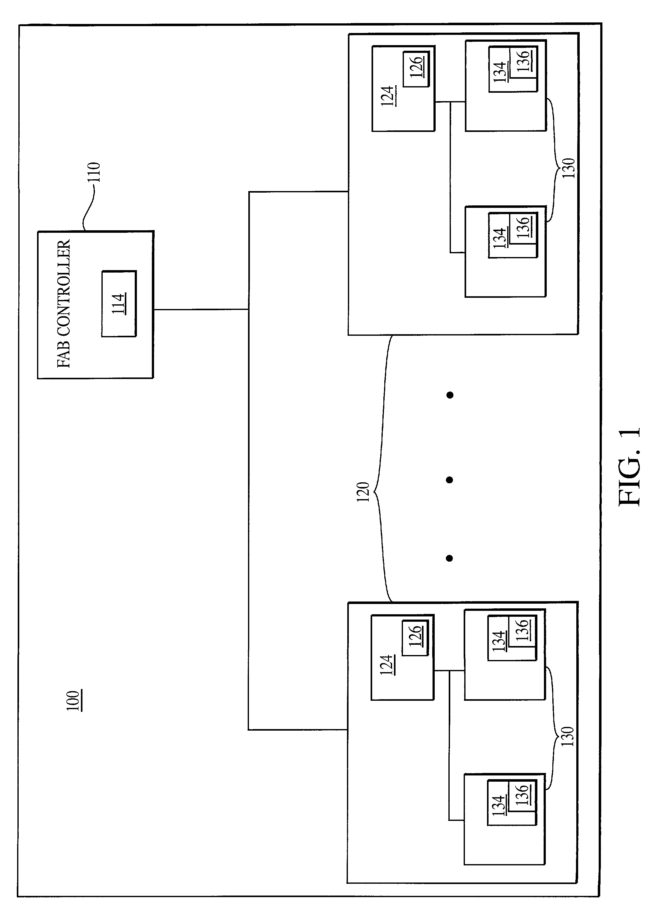
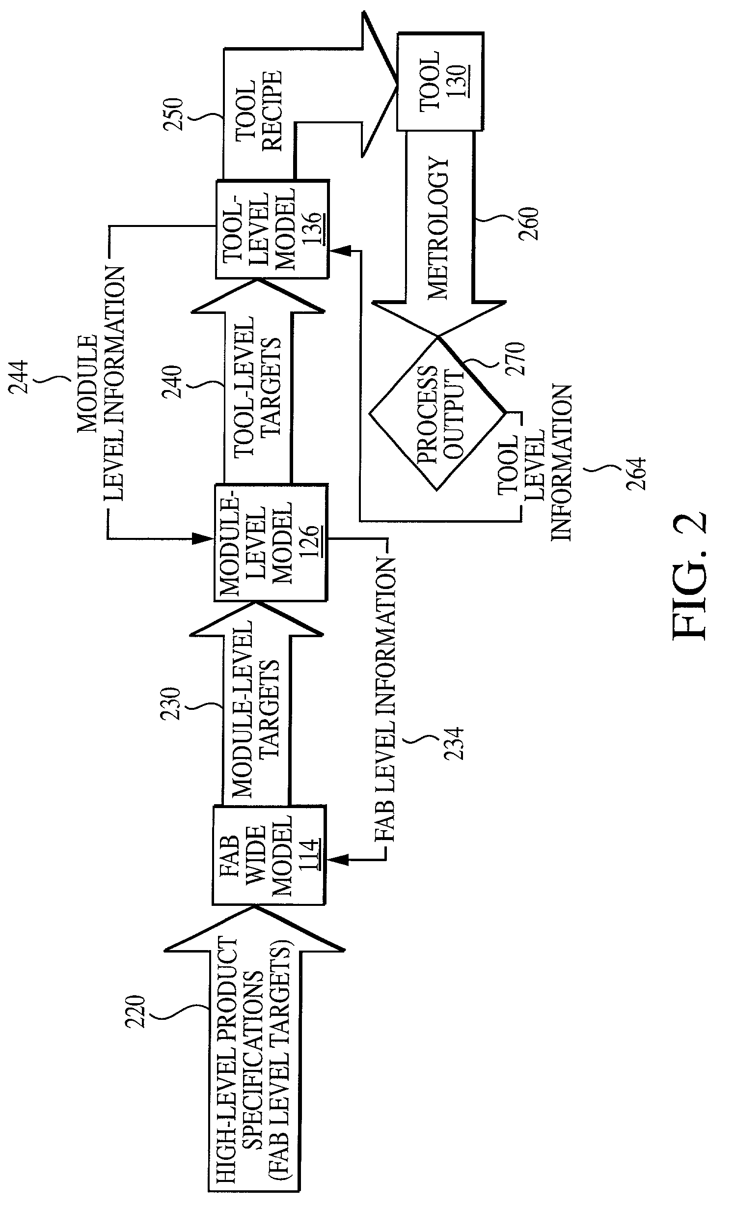
[0022]In accordance with one or more embodiments of the present invention, semiconductor wafers are processed in a fab in a manner that integrates control at multiple functional unit levels. Examples of these levels of functional units include fabs, modules, tools, and the like. Examples of modules include physical vapor deposition (PVD) modules, copper wiring modules, dep-etch modules, etc. Examples of tools include chemical vapor deposition (CVD), chemical mechanical planarization (CMP), etch, copper barrier seed, tools etc. According to one or more embodiments of the present invention, any number of functional unit property targets are initially received at a functional unit. Examples of these targets include a set of electrical parameters associated with a product, thickness uniformity, sheet resistance, film thickness, uniformity profiles, trench depth, etc. The functional unit property targets are utilized to generate a number of tool targets for any number of tool level funct...


PUM


Abstract

Semiconductor wafers are processed in a fab in a manner that integrates control at multiple functional unit levels. Examples of functional units include fabs, modules, tools, and the like. Initially, a number of functional unit property targets are received at a functional unit. The functional unit property targets are utilized to generate a number of tool targets for any number of tool level functional units. From there, the tool targets are forwarded to the corresponding tool level functional units. At these tool level functional units, a number of tool recipes, each of which define a number of process setpoints, may be generated by processing the tool targets. The process setpoints define a number of parameters which must be satisfied in order to attain the corresponding tool targets. In addition, in at least some embodiments, the tool targets and tool recipes are determined utilizing feedback information including functional unit states and measurements of controlled parameters.

Description

CROSS REFERENCE TO RELATED APPLICATION[0001]This application claims the benefit of U.S. Provisional Applications 60 / 298,878 and 60 / 365,770, filed respectively on Jun. 19, 2001 and Mar. 21, 2002, both of which are incorporated herein by reference.FIELD OF THE INVENTION[0002]The present invention relates generally to semiconductor manufacture. More particularly, the present invention relates to techniques for integrating tool, module, and fab level control in a semiconductor manufacturing process.BACKGROUND OF THE INVENTION[0003]Present-day semiconductor wafer fabrication factories (or ‘fabs’) are extremely complex environments that require an extraordinary amount of coordination. For example, a typical fab may consist of hundreds of wafer processing tools, each of which may be responsible for performing one or more of a variety of operations or processes. Thus, where a wafer is processed into items such as logic (e.g., central processing units) or memory (e.g., DRAMs), each tool perf...

Claims


Application Information

Patent Timeline
IPC IPC(8): G06F19/00B24B49/18B24B53/007B24B53/017G05B19/418H01L21/00H01L21/66
CPCB24B49/18B24B53/017G05B19/41865H01L22/20H01L21/67276G05B2219/32053G05B2219/45031H01L21/67253G05B2219/32065Y02P90/02
Inventor SHANMUGASUNDRAM, ARULKUMAR P.SCHWARM, ALEXANDER T.
Owner APPLIED MATERIALS INC
Why Eureka
Try Eureka