
Method of making a multilayer wiring board

a multi-layer wiring and wiring board technology, applied in the direction of printed circuit non-printed electric components, semiconductor/solid-state device details, instruments, etc., can solve the problems of difficult to obtain a built-in component type multi-layer wiring board of high reliability, glass cloth included in the prepreg material interferes with (occupies space for) the electronic component, etc., to achieve the effect of simplifying the manufacturing process

Inactive Publication Date: 2006-05-23
FUJITSU LTD
View PDF14 Cites 14 Cited by
  • Summary
  • Abstract
  • Description
  • Claims
  • Application Information

AI Technical Summary

Benefits of technology

[0014]A first object of the present invention is to provide a built-in component type multilayer wiring board that can be manufactured by simplified manufacturing processes and a manufacturing method thereof.
[0018]Additionally, according to another aspect of the present invention, in the above-mentioned multilayer wiring board, the frame resin layer may include glass cloth as a frame and a resin surrounding the glass cloth may be completely cured.
[0020]According to the above-mentioned aspects of the present invention, the frame resin layer having a preachieved rigidity maintains the form of the multilayer wiring board, and the electronic components are buried in the resin layer. Thus, the multilayer wiring board according to the present invention can be manufactured without processes such as hollowing out prepreg material and adjusting the position of a hollowed out part (space) as in the conventional case. Therefore, it is possible to simplify the processes and to manufacture the multilayer wiring board with a low cost.
[0023]According to the above-mentioned aspects of the present invention, it is possible to manufacture the multilayer wiring board including the frame resin layer having a preachieved rigidity and maintaining the form of the multilayer wiring board and the resin layer including the electronic components buried therein without including processes such as hollowing out the material and adjusting the position of the space. Thus, according to the manufacturing method of the multilayer wiring board according to the present invention, it is possible to simplify the processes and to manufacture the multilayer wiring board at a low cost compared with the conventional method.
[0029]According to the above-mentioned aspects of the present invention, a test on the incomplete multilayer wiring board may be also performed in addition to a local test on each component and a test on the complete multilayer wiring board. Thus, it is possible to improve the yield of the complete multilayer wiring board and to lower the manufacturing cost thereof.

Problems solved by technology

However, the manufacturing process of the built-in component type multilayer wiring board is complex.
Accordingly, it is difficult to obtain a built-in component type multilayer wiring board of high reliability.
The glass cloth included in the prepreg material interferes with (occupies space for) the electronic component.
Therefore, it is not possible to perform adequate electrical testing.
Additionally, when the finished multilayer wiring board includes a defect, it is difficult to fix the defect.
Further, the defective rate increases drastically since the multilayer wiring board includes many layers and components.
As a result, the manufacturing cost increases.

Method used


Image

  • Method of making a multilayer wiring board
  • Method of making a multilayer wiring board
  • Method of making a multilayer wiring board

Examples


Embodiment Construction

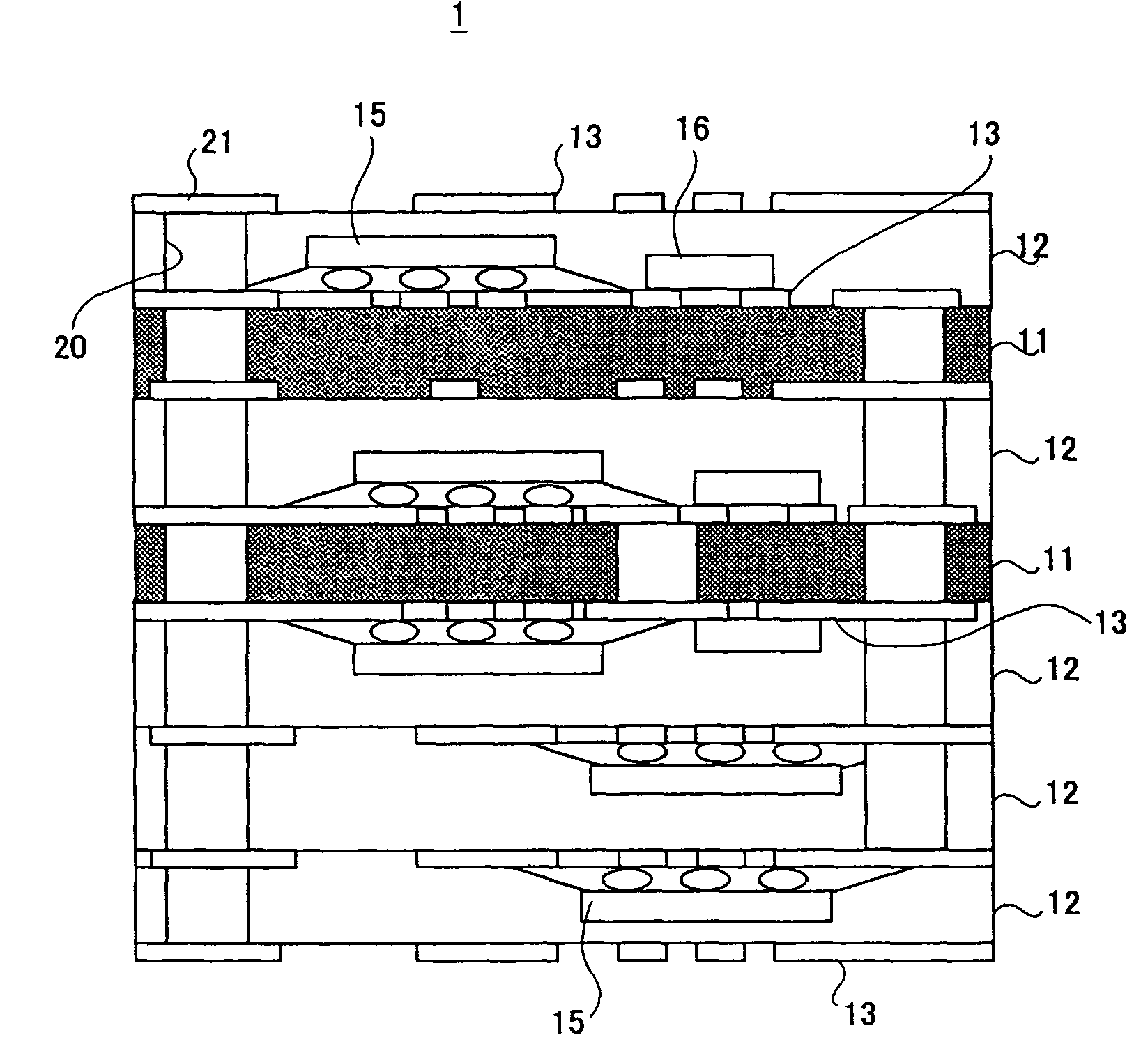
[0037]A description will be given of embodiments of the present invention, by referring to the drawings. FIG. 3 is a schematic diagram showing a general structure of a built-in electronic component type multilayer wiring board 1 according to an embodiment of the present invention.

[0038]In FIG. 3, a frame resin layer 11 corresponds to a conventional base board. The frame resin layer 11 has rigidity to maintain the form of the multilayer wiring board 1. The frame resin layer 11 is a completely cured resin layer including at least one of glass cloth, filler, and nonwoven fabric, for example.

[0039]More specifically, the frame resin layer 11 is completely cured including glass cloth as its frame and resin surrounding the glass cloth. Additionally, fragments of filler or nonwoven fabric may be further included in the resin. Further, the frame resin layer 11 may not include glass cloth but include fragments of filler or nonwoven fabric. The frame resin layer 11 may have the desired rigidit...


PUM

PropertyMeasurementUnit
distancesaaaaaaaaaa
areaaaaaaaaaaa
rigidityaaaaaaaaaa

Abstract

A built-in component type multilayer wiring board includes at least one resin layer and at least one frame resin layer. The resin layer includes electronic components buried therein. The frame resin layer includes at least one of glass cloth, filler and nonwoven fabric. The frame resin layer includes no electronic component.

Description

[0001]This Application is a Division of Ser. No. 10 / 274,125, filed 21 Oct. 2002, now abandoned.BACKGROUND OF THE INVENTION[0002]1. Field of the Invention[0003]The present invention relates to a multilayer wiring board formed by stacking a plurality of boards mounting electronic components such as a coil, a condenser and an IC chip.[0004]2. Description of the Related Art[0005]It is possible for a multilayer wiring board having electronic components within its layers (referred to as “built-in component type multilayer wiring board”, hereinafter) to correspond to speeding up of a signal since distances between the components can be reduced. The built-in component type multilayer wiring board can mount the same components as those of a conventional single layer board using an area smaller than that required by the conventional single layer board. Such a built-in component type multilayer wiring board is useful as a printed wiring board unit. Thus, many examinations of the built-in compo...

Claims


Application Information

Patent Timeline
Patent Type & Authority Patents(United States)
IPC IPC(8): H05K3/30G01R31/02G01R31/28H01L23/14H01L23/538H01L25/065H05K1/18H05K3/46
CPCG01R31/2806H01L25/0657H05K1/186H05K3/4614H01L23/145Y10T29/49117H01L23/5385H01L2225/06517H01L2225/0652H01L2225/06541H01L2225/06572H01L2225/06596H01L2924/01078H01L2924/19105H05K2203/061H05K2203/162H01L2224/16225H01L2224/32225H01L2224/73204Y10T29/49128Y10T29/49126Y10T29/49144Y10T29/49133Y10T29/49004Y10T29/4913Y10T29/49002H01L2924/00012H01L2924/1627
Inventor NAKAMURA, NAOKI
Owner FUJITSU LTD
Learn More