Method for fabricating semiconductor package and semiconductor package

a technology of semiconductor and semiconductor shell, applied in the manufacture of multilayer circuits, semiconductor devices, semiconductor/solid-state devices, etc., can solve the problems of difficult mechanical processing, unnecessarily forming plated nickel/gold coating layers at through holes, and often damaged previously formed circuit patterns

Inactive Publication Date: 2006-05-23
LG ELECTRONICS INC +1
View PDF3 Cites 96 Cited by
  • Summary
  • Abstract
  • Description
  • Claims
  • Application Information

AI Technical Summary

Benefits of technology

[0015]To further achieve at least the above objects in whole or in parts and in accordance with the purpose of the invention, as embodied and broadly described herein, a method for fabricating a semiconductor package, including forming a plurality of circuit patterns, forming a cavity in a central portion of each of the plurality of circuit patterns, mounting a semiconductor chip within the cavity, and forming a bonding pad circuit pattern to be connected to the semiconductor within the cavity, wherein a first coating layer is formed with a non-copper metal material at the bonding pad circuit pattern and a copper plating is formed on the first coating layer.
[0015]To further achieve at least the above objects in whole or in parts and in accordance with the purpose of the invention, as embodied and broadly described herein, a method for fabricating a semiconductor package, including forming a plurality of circuit patterns, forming a cavity in a central portion of each of the plurality of circuit patterns, mounting a semiconductor chip within the cavity, and forming a bonding pad circuit pattern to be connected to the semiconductor within the cavity, wherein a first coating layer is formed with a non-copper metal material at the bonding pad circuit pattern and a copper plating is formed on the first coating layer.

Problems solved by technology

However, such a fabrication method makes it difficult to mechanically process.
Additionally, previously formed circuit patterns are often damaged in this process due to impacts or other effects occurring during the process.
Also, the plated nickel / gold coating layer is unnecessarily formed at the through hole.
However, also in this method, the lowermost substrate is subjected to processing and this method does not completely remove the organic substances filled in the cavity.
Thus, since the organic substrates remaining in the cavity works as a foreign material when the nickel / gold coating layer is formed at the bonding portion, it deteriorates the quality of a semiconductor package.

Method used


Image

  • Method for fabricating semiconductor package and semiconductor package
  • Method for fabricating semiconductor package and semiconductor package
  • Method for fabricating semiconductor package and semiconductor package

Examples


Embodiment Construction

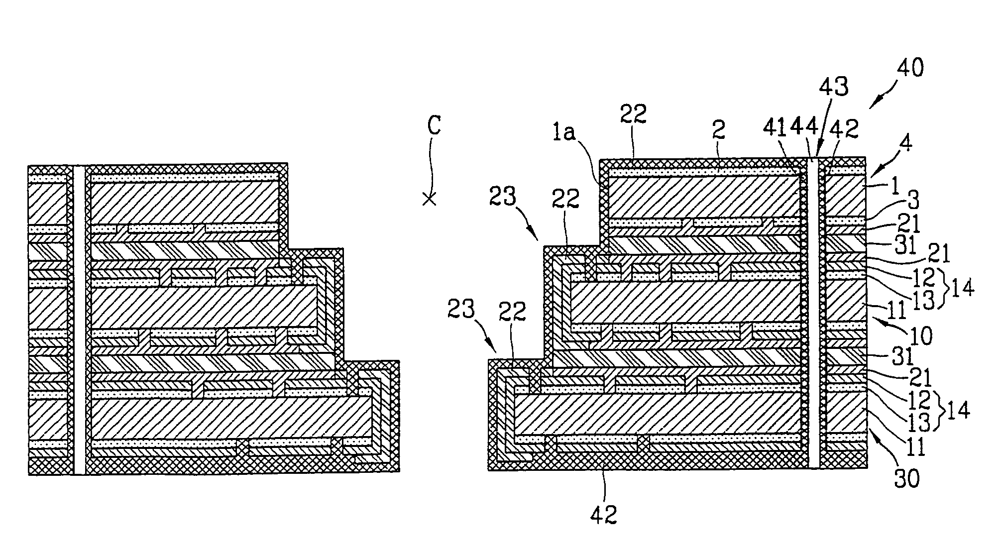
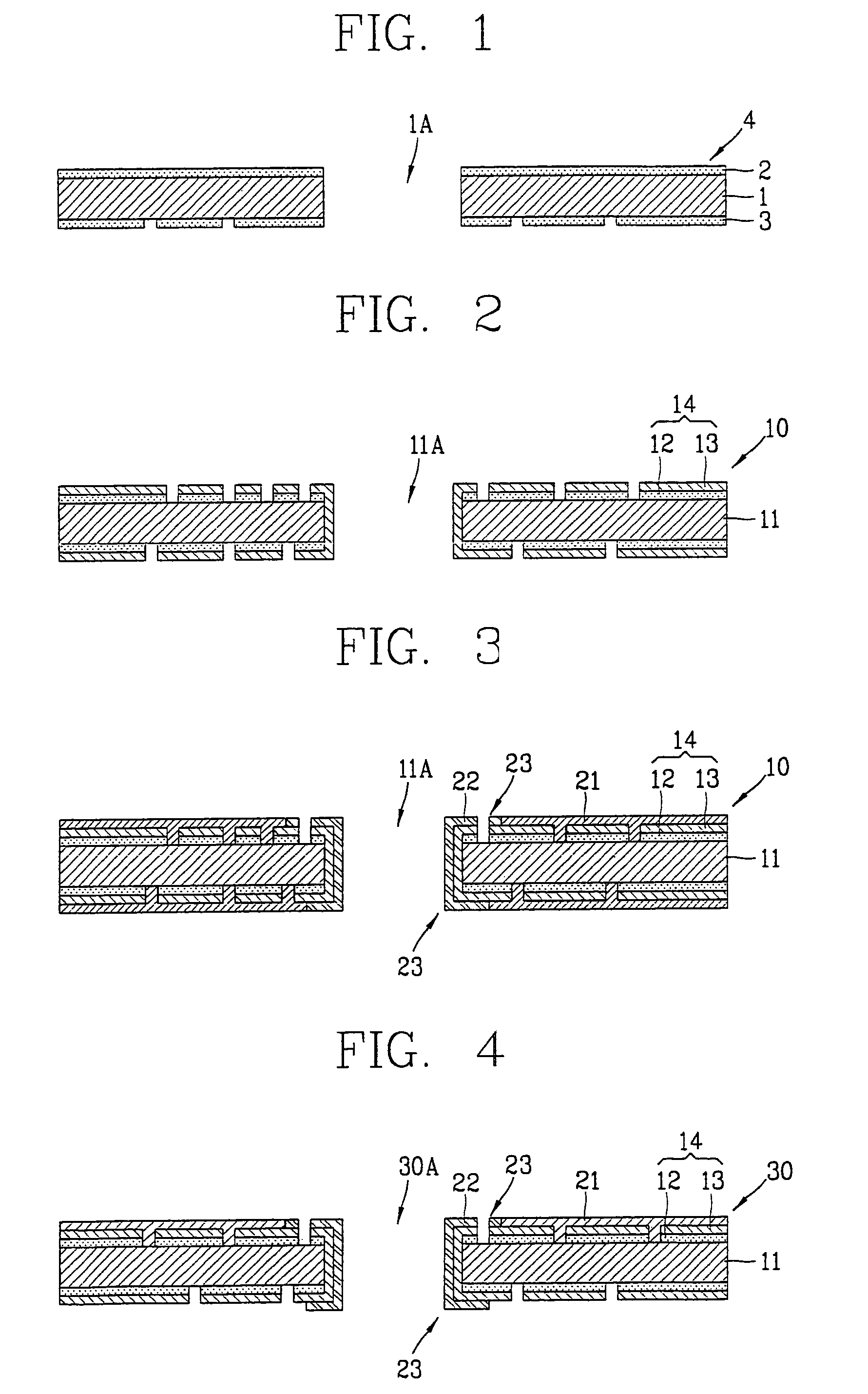
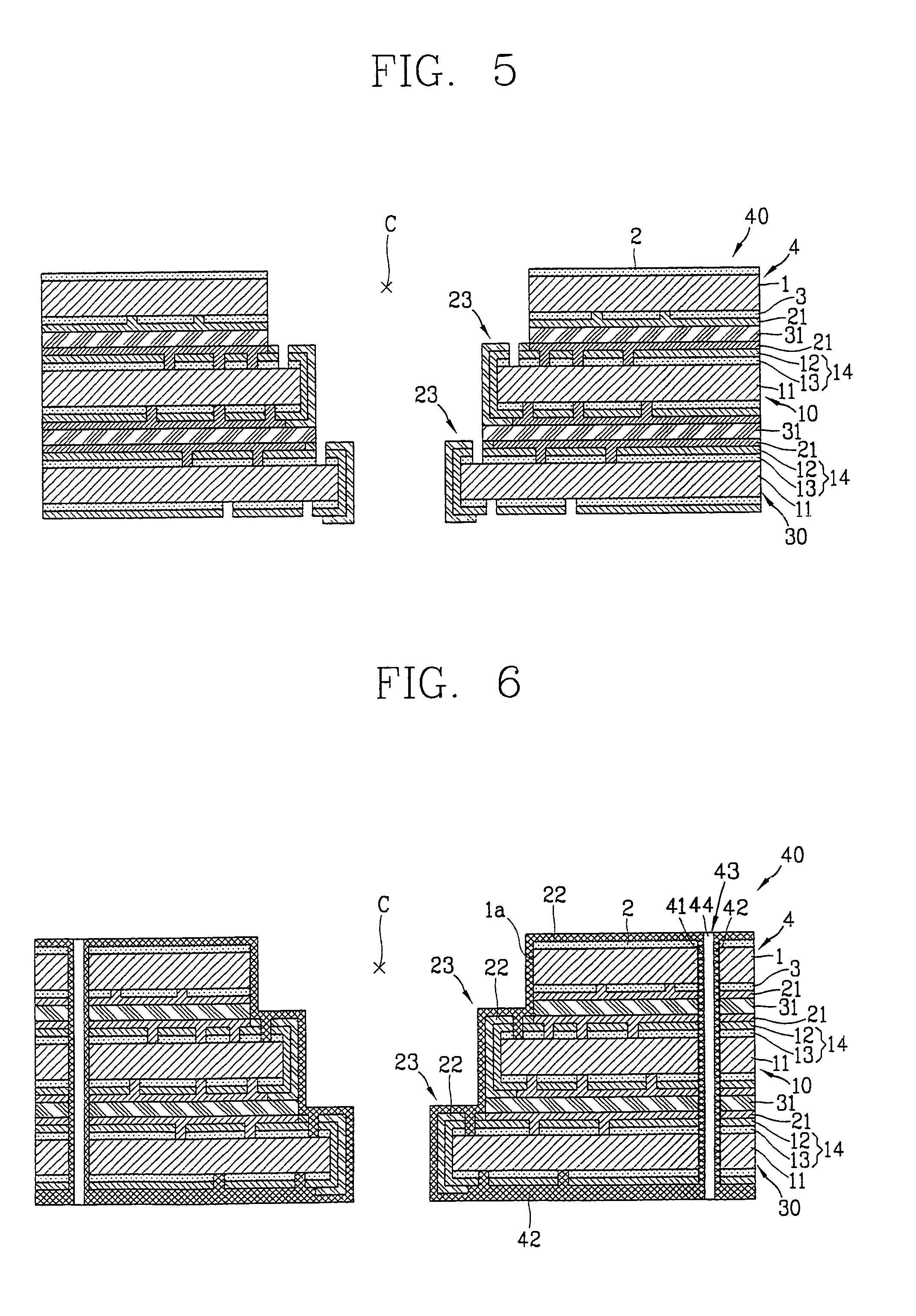
[0034]A method of fabricating a semiconductor package in accordance with an embodiment of the present invention improves the process of laminating substrates in fabricating a highly integrated package. In this embodiment, a first Ni—Au plating is formed on a bonding pad for connection with a semiconductor chip without using a mechanical process or a masking operation. This process includes applying a copper plating simultaneously on a through bore and a bonding pad, then selectively removing portions of the copper plated layer formed on the bonding pad, and then forming a second Ni—Au plating on the bonding pad and a ball pad. This process reduces the occurrences of defects due to generation of foreign material which affect masking process.

[0035]As shown in FIG. 1, first, a plated copper 2 is formed on upper and lower surfaces of an insulation substrate 1. Alternatively, a copper clad laminate (CCL) with a copper foil attached on the upper and lower surfaces of the insulation substr...


PUM


Abstract

A method of fabricating a semiconductor package is disclosed in which a first Ni—Au plating is formed on a bonding pad for connection with a semiconductor chip, without a mechanical process or a masking operation. The method applies a copper plating on a through bore and the bonding pad, where the copper plated layer formed on the bonding pad is selectively removed, and then a second Ni—Au plating is formed on the bonding pad and a ball pad.

Description

[0001]This application is a Divisional Application of U.S. patent application Ser. No. 10 / 318,303 filed Dec. 13, 2002 now U.S. Pat. No. 6,706,564 B2, which claims the benefit of Korean Patent Application No. 80826 / 2001 filed on Dec. 18, 2001, whose entire disclosures are incorporated herein by reference herein.BACKGROUND OF THE INVENTION[0002]1. Field of the Invention[0003]The present invention relates to a semiconductor package and a fabrication method thereof.[0004]2. Background of the Related Art[0005]A multi-layer substrate can be used for semiconductor packages, such as a PPGA PKG (Plastic Pin Grid Assay Package), a PBGA PKG (Plastic Ball Grid Array Package), a PLGA PKG (Plastic Pin Land Grid Array Package), or the like. The multi-layer substrate is often formed such that a substrate with a certain circuit pattern is insulatedly laminated to multiple layers and the laminated substrates are electrically connected between circuit patterns of each substrate by a through hole.[0006...

Claims


Application Information

Patent Timeline
Patent Type & Authority Patents(United States)
IPC IPC(8): H01L21/44H01L21/50H01L21/58H01L23/12H01L21/48H01L23/498H05K3/46
CPCH01L21/4857H01L23/49816H01L23/49833H01L24/49H01L2224/73265H01L2224/32245H01L2924/014H01L2924/01023H01L24/48H01L2924/1532H01L2924/15311H01L2924/1517H01L2924/15153H01L2924/12044H01L2924/01082H01L2924/01079H01L24/45H01L2224/45144H01L2224/48091H01L2224/48227H01L2224/48464H01L2224/49109H01L2924/01004H01L2924/01005H01L2924/01006H01L2924/01015H01L2924/01028H01L2924/01029H01L2924/01033H01L2924/01078H01L2924/00014H01L2924/00H01L2924/00012H01L24/73H05K3/46
Inventor KIM, YONG ILLEE, SUNG GUEYANG, YU SEOCK
Owner LG ELECTRONICS INC
Why Eureka
Try Eureka