Stacked semiconductor device

a semiconductor device and stacked technology, applied in the field of stacking semiconductor devices, can solve the problems requiring considerable manufacturing processes, and high manufacturing costs, and achieves the effects of increasing manufacturing costs, increasing manufacturing costs, and increasing manufacturing costs

Active Publication Date: 2006-05-23
SOCIONEXT INC
View PDF5 Cites 273 Cited by
  • Summary
  • Abstract
  • Description
  • Claims
  • Application Information

AI Technical Summary

Benefits of technology

[0025]Accordingly, the present invention provides a stacked semiconductor device that substantially obviates one or more of the problems caused by the limitations and disadvantages of the related art.

Problems solved by technology

Nevertheless, according to the semiconductor device disclosed by the patent reference 1, problems are that no more than one semiconductor device unit can be stacked beneath (i.e., two in total), and that a terminal has to be prepared at the upper part of the package by deforming a leadframe, requiring considerable manufacturing processes, with manufacturing cost becoming high.
According to the semiconductor device disclosed by the patent reference 2, problems are that the stacked end product becomes thick since each semiconductor device unit is molded, and considerable manufacturing processes are required in order to form the penetration wiring, raising manufacturing cost.
In this case, a problem is in that the external connection terminals of each semiconductor device unit are not necessarily set up such that stacking can be carried out.

Method used


Image

  • Stacked semiconductor device
  • Stacked semiconductor device
  • Stacked semiconductor device

Examples


first embodiment

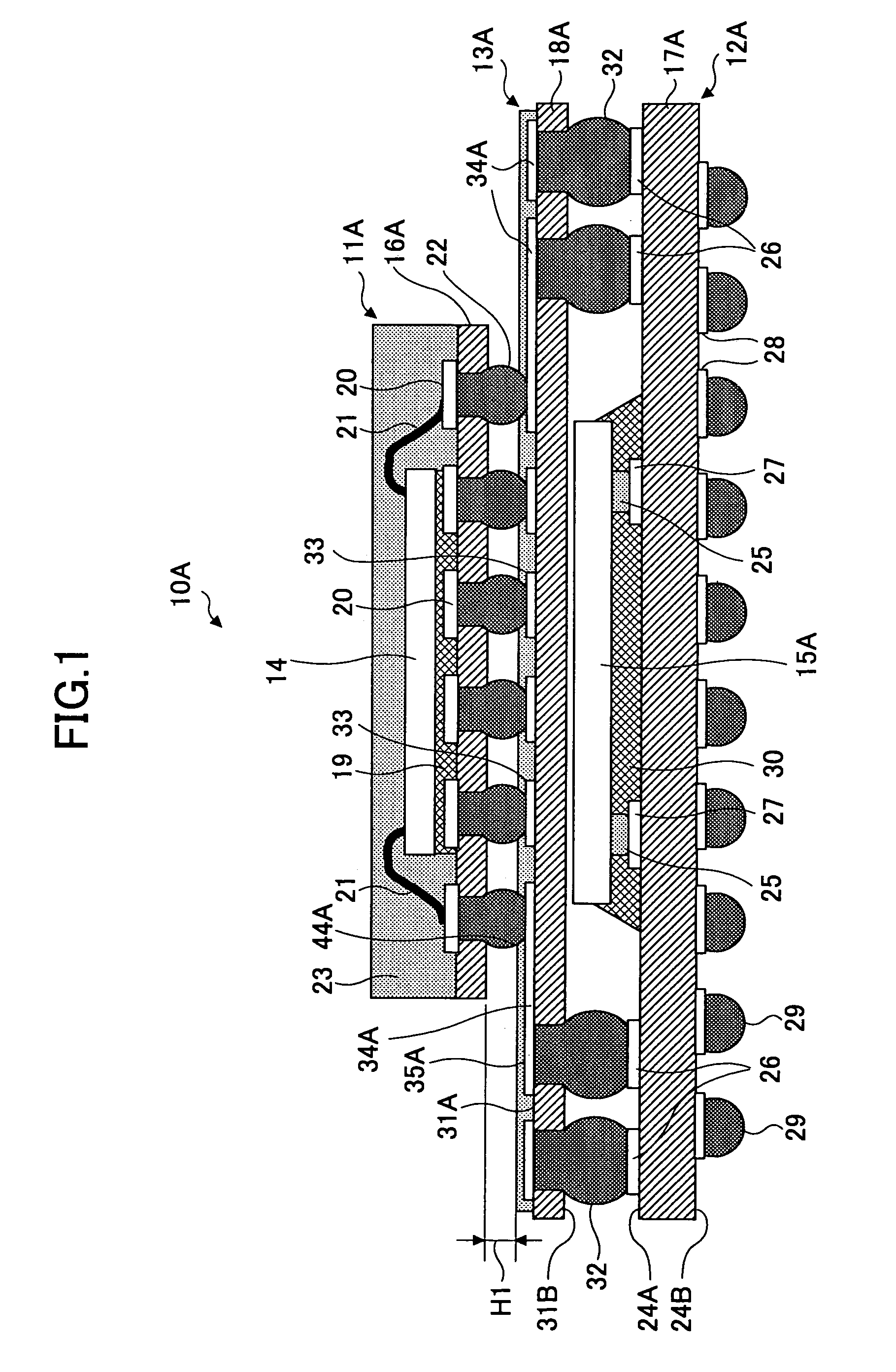
[0034]FIG. 1 shows a stacked semiconductor device (henceforth referred to as “semiconductor device”) 10A according to the present invention. The semiconductor device 10A includes an upper semiconductor device unit 11A (henceforth called “upper device unit”), a lower semiconductor device unit 12A (henceforth called “lower device unit”), and an interposer substrate 13A.

[0035]The upper device unit 11A is a general-purpose semiconductor device that is commercially available. That is, a commercial product that is guaranteed by a manufacturer is used as the upper device unit 11A.

[0036]Further, the device unit 11A is a BGA (Ball Grid Array) type semiconductor device wherein a semiconductor element 14A is mounted on the upper surface of a first wiring substrate 16A, and external connection terminals 22 are arranged on the undersurface of the first wiring substrate 16A. A solder ball constitutes each of the external connection terminals 22.

[0037]According to the present embodiment, the semic...

second embodiment

[0054]Next, the present invention is explained.

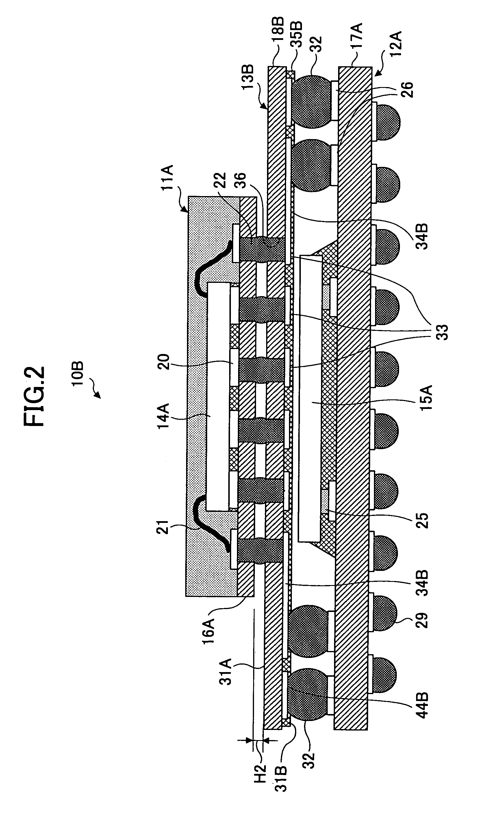
[0055]FIG. 2 shows a semiconductor device 10B according to the second embodiment of the present invention. In FIG. 2 that is for explaining the second embodiment and FIGS. 3 through 7 that are for explaining subsequent embodiments, the same label is used for the same component as shown in FIG. 1, and explanation thereof is not repeated.

[0056]The semiconductor device 10B of the present embodiment includes the upper device unit 11A and the lower device unit 12A, which are the same as in the semiconductor device 10A of the first embodiment. However, the semiconductor device 10B of the present embodiment includes an interposer substrate 13B that is different from the interposer substrate 13A of the first embodiment. In the case of the interposer substrate 13A of the first embodiment, both second conductive members 33 and third conductive members 34A are formed on the upper surface 31A of the circuit board 18A. Conversely, in the case of the...

third embodiment

[0063]Next, the present invention is explained.

[0064]FIG. 3 shows a semiconductor device 10C according to the third embodiment of the present invention. The semiconductor device 10C includes the upper device unit 11A and the lower device unit 12A, which are the same as in the semiconductor device 10A of the first embodiment. However, an interposer substrate 13C of the semiconductor device 10C is different from the first and the second embodiments.

[0065]In the cases of the interposer substrates 13A and 13B, the third conductive members 34A and 34B, respectively, are provided on the upper surface 31A and the undersurface 31B, respectively, of the circuit board 18A and 18B, respectively, i.e., only on one of the surfaces.

[0066]Conversely, in the case of the interposer substrate 13C of the present embodiment, the third conductive members 34A and 34B are provided on upper surface 31A and undersurface 31B, respectively. Specifically, the third conductive members 34A and the second conduct...


PUM


Abstract

A stacked semiconductor device is disclosed that has a three-dimensional structure using general-purpose semiconductor device units (semiconductor devices) that are stacked with an interposer substrate being provided between an upper device unit and a lower device unit. The upper device unit includes a semiconductor device, a first wiring substrate, and an external connection terminal. The lower device unit includes a semiconductor device, a second wiring substrate, and a connection electrode that is prepared on the upper surface of the second wiring substrate. The interposer substrate includes a circuit board, a first conductive material connecting to the connection electrode, a second conductive material formed in a form position of the external connection terminal that is electrically connected to the second conductive material, and a third conductive material for electrically connecting the first conductive material and the second conductive material.

Description

BACKGROUND OF THE INVENTION[0001]1. Field of the Invention[0002]The present invention generally relates to a stacked semiconductor device, and especially relates to a stacked semiconductor device having a three-dimensional structure wherein two or more semiconductor device units and semiconductor devices are stacked.[0003]With advancement of electronic apparatuses in recent years, semiconductor devices used therein are increasingly required to be small in size, thin, capable of providing multiple functions and advanced features, and highly condensed. In order to meet such requirements, the packaging structure of semiconductor devices is shifting to a three-dimensional structure wherein two or more semiconductor device units or two or more semiconductor devices are stacked.[0004]2. Description of the Related Art[0005]Conventionally, semiconductor devices with three-dimensional structures containing two or more semiconductor device units have been disclosed as JPL, 06-252334 (pp. 3 th...

Claims


Application Information

Patent Timeline
Patent Type & Authority Patents(United States)
IPC IPC(8): H01L23/02H01L25/18H01L23/31H01L25/065H01L25/10H01L25/11H05K1/02H05K1/14H05K1/16H05K3/34
CPCH01L23/3128H01L25/0657H01L25/16H05K1/141H01L25/105H01L2224/32225H01L2225/107H01L2225/1058H01L2225/1023H01L24/48H05K2201/10734H05K2201/10515H05K2201/049H05K2201/045H05K3/3436H05K1/16H05K1/145H05K1/144H05K1/023H01L2924/19105H01L2924/19041H01L2924/15331H01L2924/15311H01L2225/06586H01L2225/06572H01L2225/06568H01L2224/16225H01L2224/32145H01L2224/48091H01L2224/48227H01L2224/73204H01L2224/73265H01L2225/0651H01L2225/06517H01L2225/0652H01L2225/06541H01L2225/06555H01L2225/06558H01L2924/00014H01L2924/00012H01L24/73H01L2224/05599H01L2224/45099H01L2224/85399H01L2924/181H01L2224/45015H01L2924/207
Inventor NISHIMURA, TAKAOAIBA, KAZUYUKITAKASHIMA, AKIRA
Owner SOCIONEXT INC
Why Eureka
Try Eureka