Optical proximity effect correcting method and mask data forming method in semiconductor manufacturing process, which can sufficiently correct optical proximity effect, even under various situations with regard to size and shape of design pattern, and space width and position relation between design patterns

a technology of optical proximity and correcting method, which is applied in the direction of counting objects on conveyors, printing, instruments, etc., can solve the problems of insufficient proximity effect correction, inability to accurately record the same shape, and inability to achieve sufficient proximity effect correction

Inactive Publication Date: 2006-06-06
RENESAS ELECTRONICS CORP
View PDF13 Cites 15 Cited by
  • Summary
  • Abstract
  • Description
  • Claims
  • Application Information

AI Technical Summary

Benefits of technology

[0014]The present invention has been made to solve the above-described problems of the conventional optical proximity effect correcting method. An object of the present invention is to provide an optical proximity effect correcting method and a mask data forming method in a semiconductor manufacturing process, which can sufficiently correct an optical proximity effect even under various situations with regard to a size and a shape of a design pattern, and a space width and a position relation between the design patterns.

Problems solved by technology

The optical proximity effect implies that exposure transcription cannot be carried out accurately in the same shape due to light interference between proximity lights adjacent to each other.
If the proximity effect is corrected under such situation, there may be a case that the sufficient proximity effect correction cannot be attained only by adding a correcting pattern having a certain shape to each of the various design patterns.
However, a method of limiting a design rule and a method of validating a design method are not still established.
Also, such limitation and validation may result in a drop of design efficiency and largely increase validation process time.
Not only the optical proximity correction is limited to electrically related structure, but also the individual shape edges are processed.

Method used


Image

  • Optical proximity effect correcting method and mask data forming method in semiconductor manufacturing process, which can sufficiently correct optical proximity effect, even under various situations with regard to size and shape of design pattern, and space width and position relation between design patterns
  • Optical proximity effect correcting method and mask data forming method in semiconductor manufacturing process, which can sufficiently correct optical proximity effect, even under various situations with regard to size and shape of design pattern, and space width and position relation between design patterns
  • Optical proximity effect correcting method and mask data forming method in semiconductor manufacturing process, which can sufficiently correct optical proximity effect, even under various situations with regard to size and shape of design pattern, and space width and position relation between design patterns

Examples


first embodiment

[0063]At first, a first embodiment is described.

[0064]This embodiment is a technique for modifying a wiring pattern in a layout data which is not yet modified, to generate a mask drawing data based on the modified wiring pattern, in accordance with the optical proximity effect correcting method of the semiconductor manufacturing process.

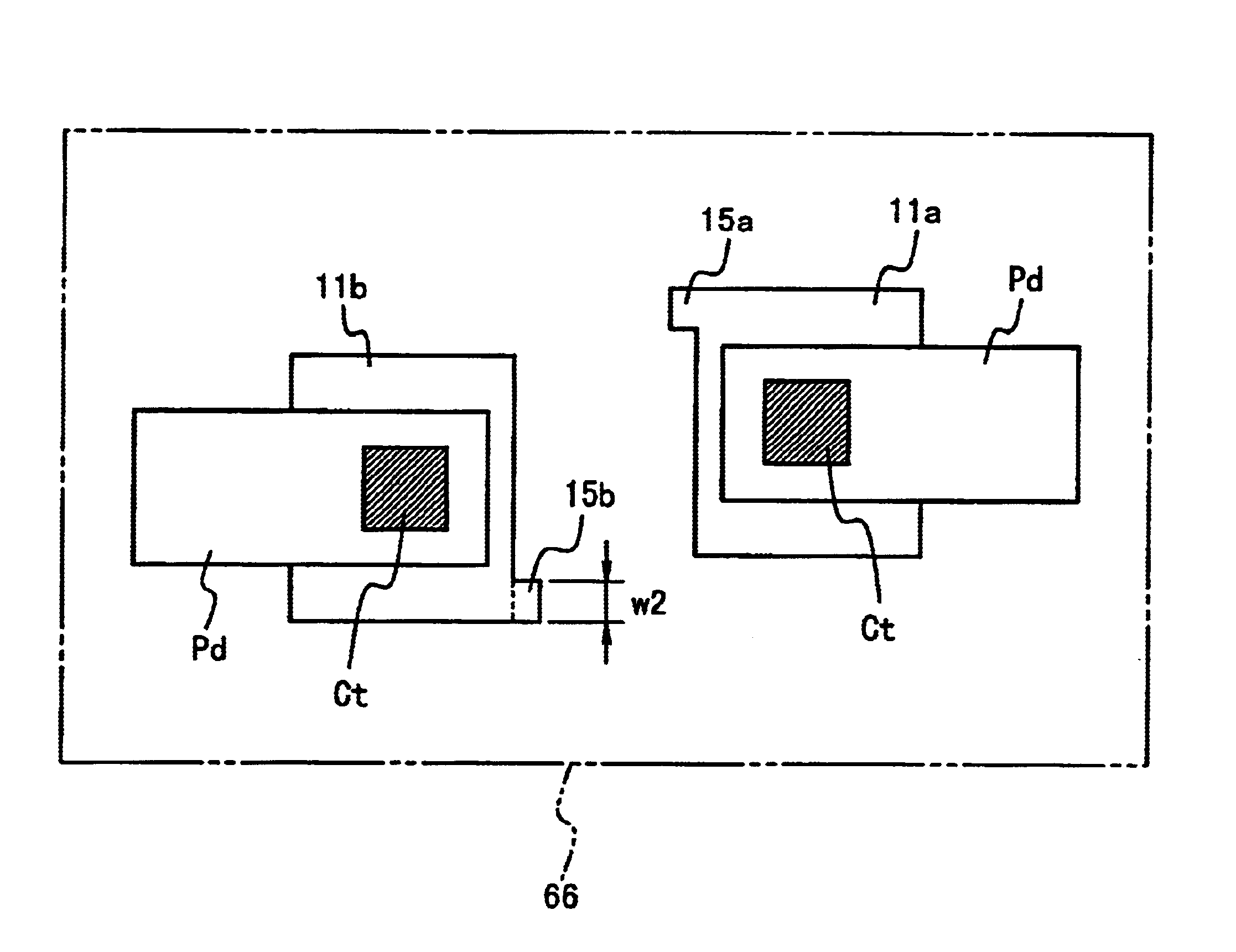
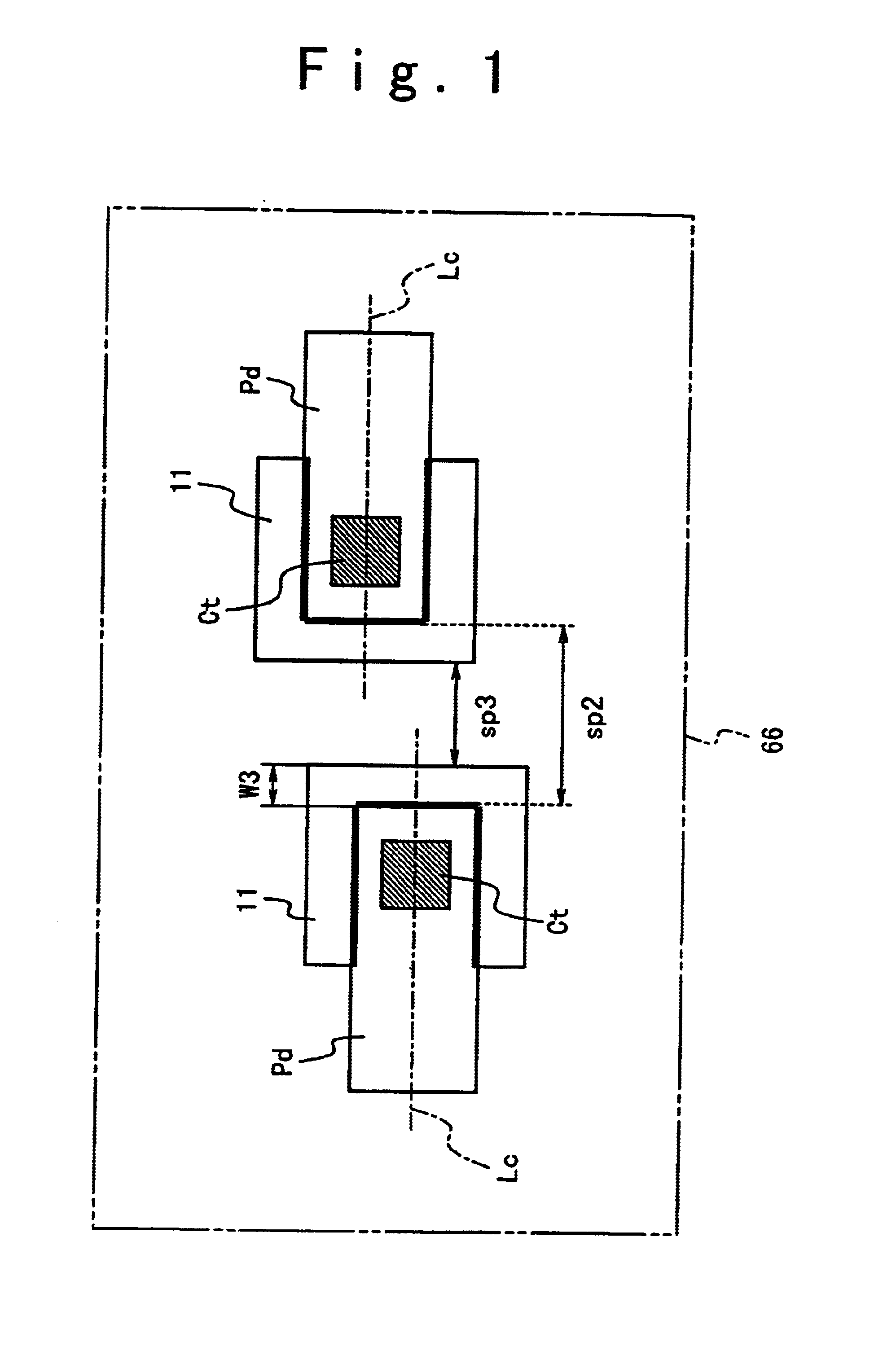
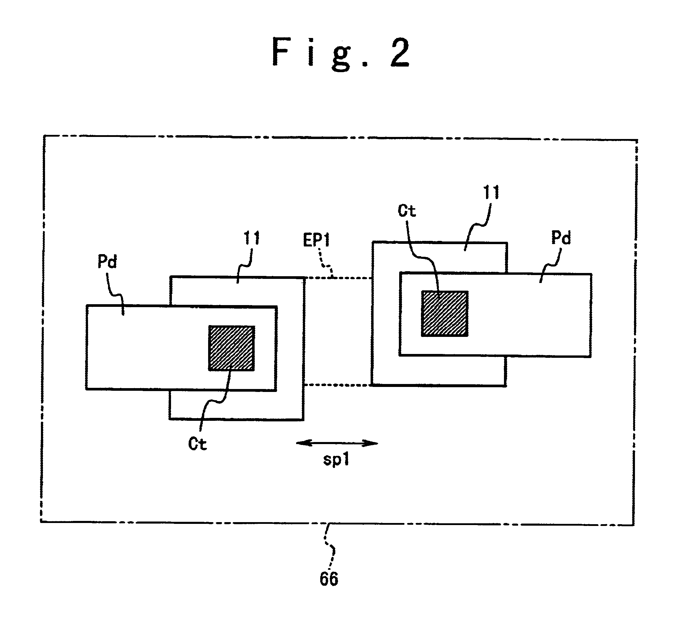
[0065]As shown in FIG. 1, a computer 66 stores therein the layout data which is not yet modified. The layout data which is not yet modified includes a wiring (design pattern) Pd which is a wiring layer pattern or an element thereof and a contact Ct which is a contact layer pattern or an element thereof.

[0066]The design pattern Pd is designed at an interval equal to or greater than a minimum space width sp2 (for example, 0.18 μm or 0.24 μm) defined in accordance with a minimum design rule. A single correcting pattern 11 having a horizontally-reclined U-shaped style when it is viewed on a flat surface is added to an end of the design pattern Pd so as t...

second embodiment

[0089]On the contrary, a correcting figure described in the second embodiment is added in view of the following background.

[0090]As shown in FIG. 12, a pattern 41 in which the contact Ct and the wiring Pd overlap with each other and a pattern 42 having only the wiring Pd are used to design the pattern, in many cases. In order to connect the contact Ct in the pattern 41 to the pattern 42 of the wiring Pd, the pattern 41 and the pattern 42 may be in contact with each other. Thus, as denoted by a symbol 43, a pattern arrangement may be considered in which only a part of the pattern 41 is projected which has a wiring width Hb different from a wiring width Ha of the wiring pattern 42 and the like. Actually, there may be a design based on such arrangement. However, this causes a pattern 43 in a form of small notch to be brought about.

[0091]The inhibition of the pattern in the form of small notch causes the number of CAD check items to be increased. Thus, this cannot be inhibited since an ...


PUM

PropertyMeasurementUnit
space widthaaaaaaaaaa
widthaaaaaaaaaa

Abstract

An optical proximity effect correcting method in a semiconductor manufacturing process includes adding, detecting, judging, and deleting. The adding includes adding a first correcting region around a portion of a first design pattern. The portion faces a second design pattern. A first corrected design pattern includes the first correcting region and the first design pattern. The detecting includes detecting a space between the first corrected design pattern and the second design pattern. The judging includes judging whether the space is smaller than or equal to a predetermined value. The deleting includes deleting at least a portion of the first correcting region such that the space is larger than the predetermined value, when the space is smaller than or equal to the predetermined value.

Description

[0001]This application is a division of Ser. No. 09 / 458,625 filed Dec. 10, 1999.BACKGROUND OF THE INVENTION[0002]1. Field of the Invention[0003]The present invention relates to an optical proximity effect correcting method and a mask data forming method in a semiconductor manufacturing process.[0004]2. Description of the Related Art[0005]In an optical lithography process of a semiconductor device manufacturing process, an optical proximity effect is incurred. The optical proximity effect implies that exposure transcription cannot be carried out accurately in the same shape due to light interference between proximity lights adjacent to each other. Therefore, it is required to reduce pattern dimension error caused by such optical proximity effect. The reduction of the pattern dimension error is compensated by correcting the proximity effect, as known in Japanese Laid Open Patent Application (JP-A-Heisei 5-80486). This correction technique is the calculation technique of modifying a li...

Claims


Application Information

Patent Timeline
Patent Type & Authority Patents(United States)
IPC IPC(8): G06F17/50H01L21/027G03F1/00G03F1/36G03F1/68G03F1/70G03F7/20
CPCG03F1/144G03F7/70441G03F1/36H01L21/027
Inventor TOUNAI, KEIICHIROHAMAMOTO, TAKESHI
Owner RENESAS ELECTRONICS CORP
Why Eureka
Try Eureka