Use of pulsed grounding source in a plasma reactor

a pulsed grounding source and plasma reactor technology, applied in the direction of plasma technique, chemical vapor deposition coating, coating, etc., can solve the problems of increasing the electric field, shortening the pedestal, and increasing the role of feature charging on the etch, so as to reduce the charge inside the feature and minimize the electrons' ability to penetrate the feature

Inactive Publication Date: 2006-06-13
MICRON TECH INC
View PDF54 Cites 34 Cited by
  • Summary
  • Abstract
  • Description
  • Claims
  • Application Information

AI Technical Summary

Benefits of technology

[0016]The present invention relates to an apparatus and method of reorienting electrons generated in a plasma reactor to minimize the electrons' ability to penetrate a feature and therefore reduce charging inside the feature.

Problems solved by technology

This results in an increase in the electric field that retards electron flow to the wafer.
In other words, the shorting of the pedestal increases the role of feature charging on the etch results.

Method used


Image

  • Use of pulsed grounding source in a plasma reactor
  • Use of pulsed grounding source in a plasma reactor
  • Use of pulsed grounding source in a plasma reactor

Examples


Embodiment Construction

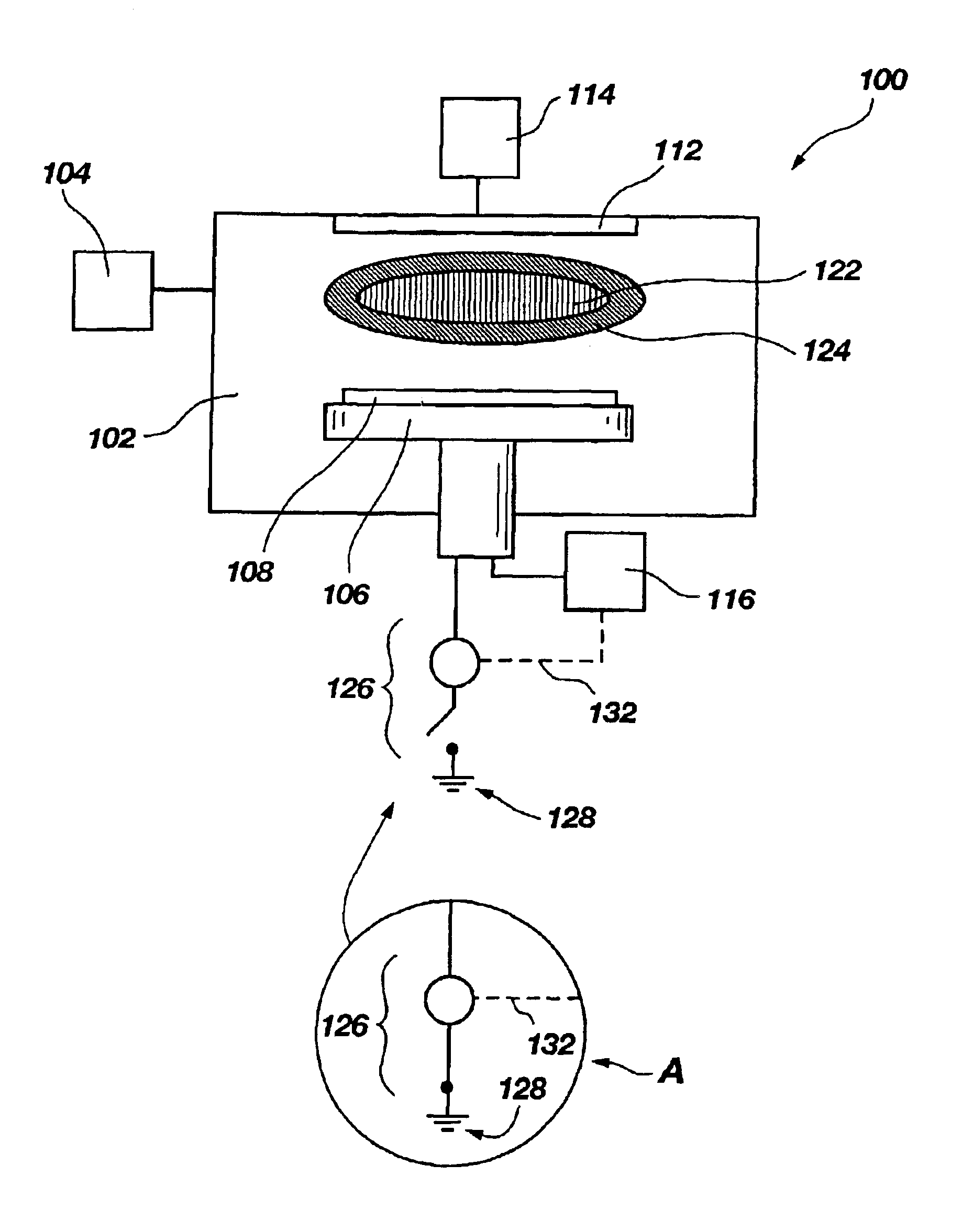
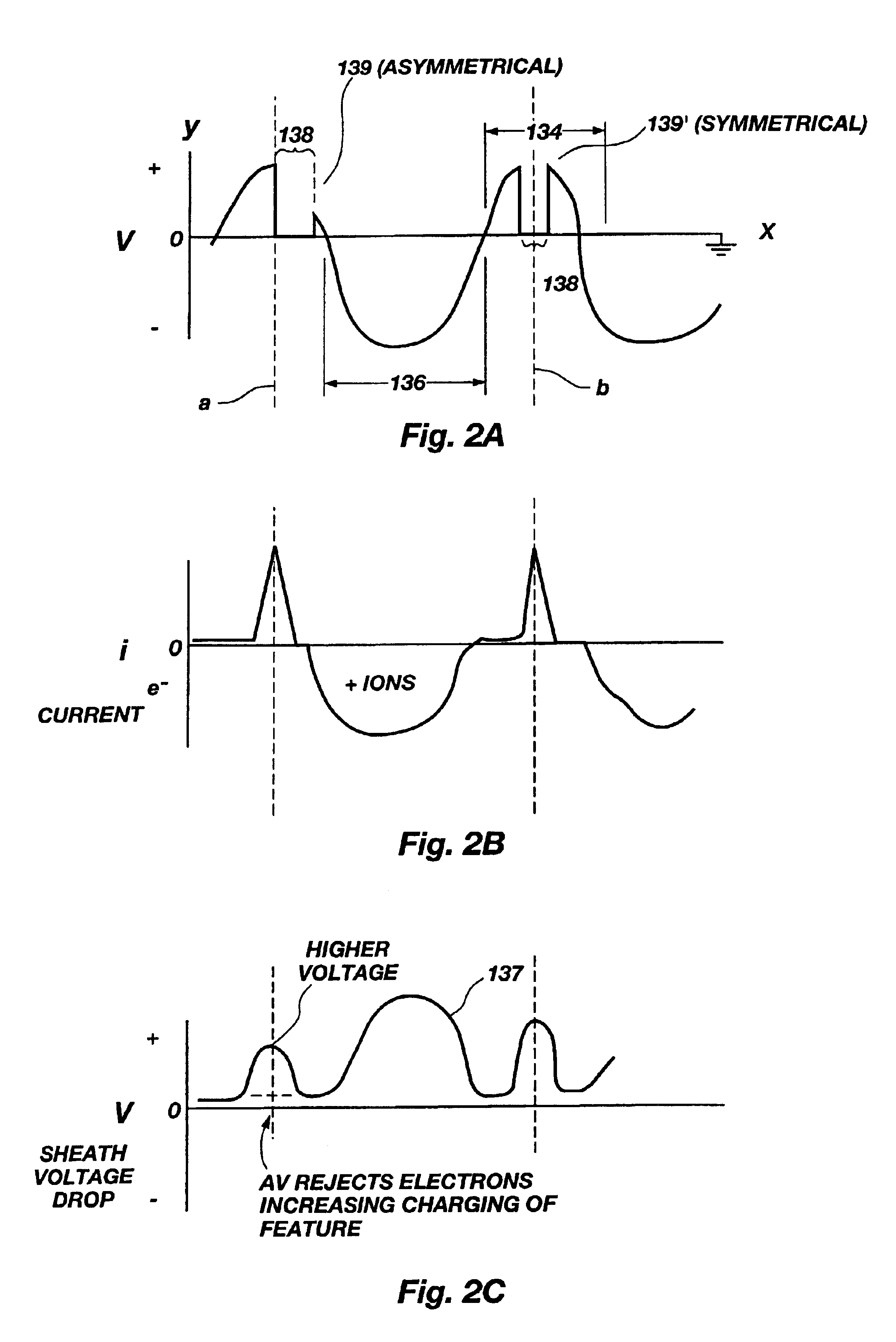
[0033]Referring to drawings FIGS. 1 through 3, illustrated are various schematics, views, and graphs of the present invention. It should be understood that the illustrations are not meant to be actual views of any particular semiconductor device, but are merely idealized representations that are employed to more clearly and fully depict the formation of contact interfaces in the present invention than would otherwise be possible. Additionally, elements common between drawing FIGS. 1 through 3 retain the same numerical designation.

[0034]As illustrated in drawing FIG. 1, one embodiment of an etching apparatus 100 of the present invention comprises an etching chamber 102 in electrical communication with a first power source 104, such as an AC power source, a microwave power source, or any suitable power source, etc. The etching chamber 102 further includes a pedestal 106 to support a semiconductor substrate 108 and an electrode 112 opposing the pedestal 106. The electrode 112, typicall...


PUM

PropertyMeasurementUnit
temperatureaaaaaaaaaa
aspect ratioaaaaaaaaaa

Abstract

A method for grounding a semiconductor substrate pedestal during a portion of a high voltage power bias oscillation cycle to reduce or eliminate the detrimental effects of feature charging during the operation of a plasma reactor.

Description

CROSS-REFERENCE TO RELATED APPLICATION[0001]This application is a divisional of application Ser. No. 09 / 649,748, filed Aug. 28, 2000, now U.S. Pat. No. 6,485,572, issued Nov. 26, 2002.BACKGROUND OF THE INVENTION[0002]1. Field of the Invention[0003]The present invention relates to plasma reactor apparatus and processes. More specifically, the present invention relates to grounding a semiconductor substrate pedestal of a plasma reactor apparatus during a portion of a positive voltage power bias oscillation cycle to increase the energy of ion particles of the plasma to increase the feature charging effects regarding a substrate being etched using the plasma reactor.[0004]2. State of the Art[0005]Higher performance, lower cost, increased miniaturization of electronic components, and greater density of integrated circuits are ongoing goals of the computer industry. One commonly used technique to increase the density of integrated circuits involves stacking multiple layers of active and p...

Claims


Application Information

Patent Timeline
Patent Type & Authority Patents(United States)
IPC IPC(8): C23C16/509C23F1/00H01L21/306H05H1/46H01J37/32H01L21/302H01L21/3065H01L21/311
CPCH01J37/32623H01J37/32706H01L21/31116H01L21/3065H01J37/32935
Inventor HEDBERG, CHUCK E.DONOHOE, KEVIN G.
Owner MICRON TECH INC
Why Eureka
Try Eureka