Device and method for spatially resolved photodetection and demodulation of modulated electromagnetic waves

a technology of modulated electromagnetic waves and devices, applied in radiation controlled devices, optical radiation measurement, instruments, etc., can solve the problems of inhomogeneity, difficult to realize four transfer gates with equal transfer efficiency, poor and slow charge transfer from the photo site to the storage site, etc., to achieve small size, reduce the effect of light power and enlarging the integration tim

Inactive Publication Date: 2006-06-13
AMS SENSORS SINGAPORE PTE LTD
View PDF8 Cites 379 Cited by
  • Summary
  • Abstract
  • Description
  • Claims
  • Application Information

AI Technical Summary

Benefits of technology

[0041]Charge carriers are repetitively added and integrated in each storage site rather than being directly fed to any post-processing electronics. This CCD charge addition ability is a nearly noise-free process and enables the system to operate with relatively low light power just by enlarging the integration times. This is an advantage over pixel realizations with in-pixel post-processing electronics.
[0042]The pixel size can be realized smaller than possible with prior art, offering a good optical fill factor (>50% even without microlens). This is possible, since storing the demodulated phase information within the pixel occupies far less space than realizing additional post-processing electronics in each pixel.

Problems solved by technology

Charge transfer from the photo site to the storage site (response / efficiency of the switch) is then relatively poor and slow.
Additionally, practice shows that it is very difficult to realize four transfer gates with equal transfer efficiencies.
Therefore, current realizations suffer from inhomogeneities between the single switch / storage combinations at practical frequencies needed for time-of-flight (TOF) applications (>1 MHz).
This is a serious restriction if TOF-measurements have to be performed of fast-changing scenes containing moving objects.
As in practical realization of DE-44 40 613 C1, this serial acquisition of an “in-phase” and “quadrature-phase” signal represents a serious drawback when being used for TOF applications with fast-changing scenes.
This access to the light sensitive area from four local different places again, as is the case in DE-44 40 613 C1, results in a non-uniform charge distribution and gives each accumulation gate a different offset, which is complicated to compensate.
Such a post-processing APS-structure, however, occupies space on the sensor and will always drastically increase the sensor's pixel size and, hence, decrease its fill factor.
Additionally, feeding the generated photocurrent directly to an amplification stage before being integrated, adds additional noise sources to the signal and decreases the structure's performance, especially for low-power optical input signals.
These optical structures, however, do not correct for local inhomogeneities in the scene detail imaged to one pixel.
Such inhomogeneities, especially to be expected due to the large pixel size, lead to measurement errors.
It is therefore not suited to be realized as a larger array of many 10,000 of pixels.
However, the increased fill factor can only be realized with larger pixels and hence the total number of pixels, which can be realized in an array, is seriously limited with the device described in this prior-art document.
That is why the measurement accuracy for targets far away from the sensor is worse than the accuracy for near targets.

Method used


Image

  • Device and method for spatially resolved photodetection and demodulation of modulated electromagnetic waves
  • Device and method for spatially resolved photodetection and demodulation of modulated electromagnetic waves
  • Device and method for spatially resolved photodetection and demodulation of modulated electromagnetic waves

Examples


Embodiment Construction

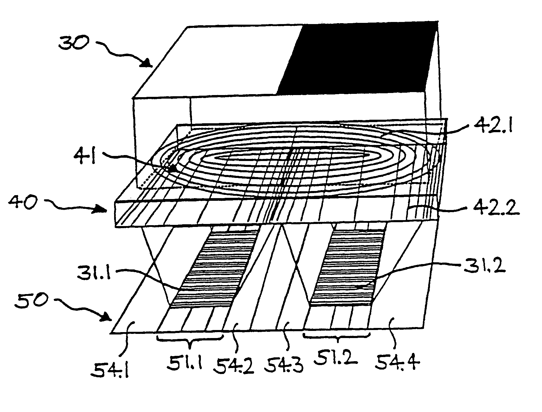
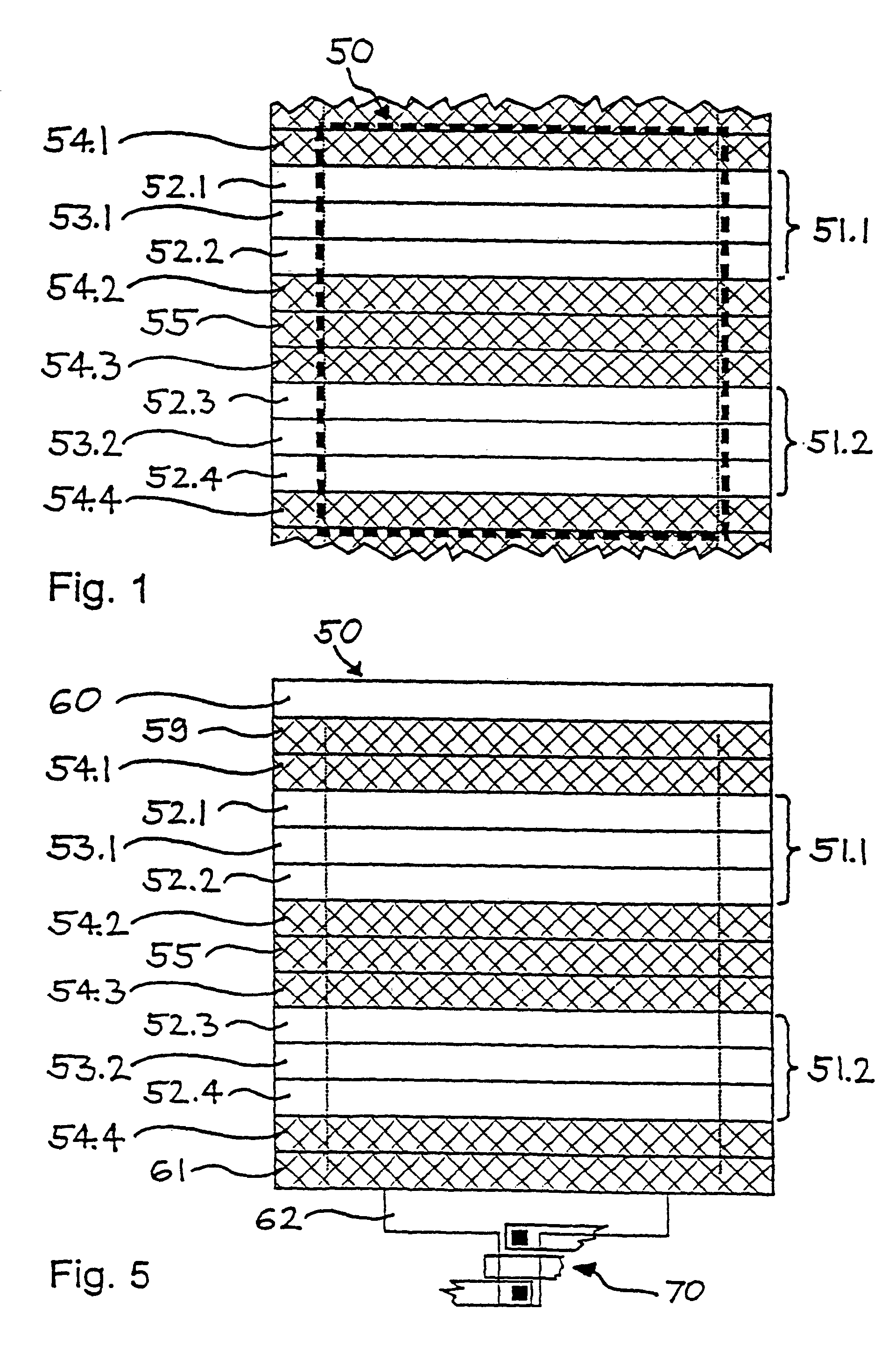
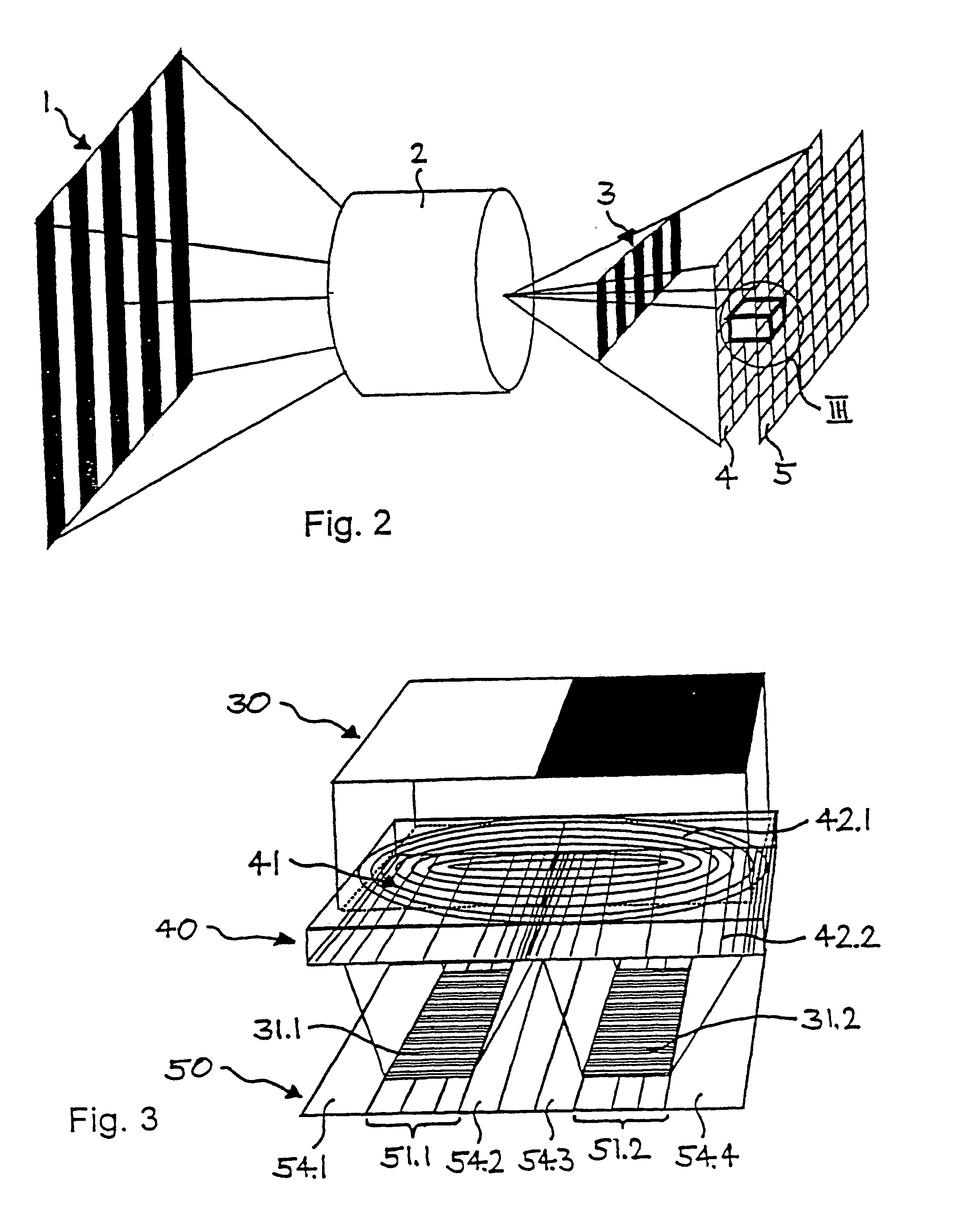
[0074]The basic structure of an exemplified pixel 50 of a device according to the invention is illustrated in FIG. 1. The pixel 50 comprises, e.g., two light-sensitive photo sites 51.1, 51.2. A first photo site 51.1 has a first photo gate 52.1 for the phase angle 0° and a second photo gate 52.2 for the phase angle 180°; a second photo site 51.2 has a third photo gate 52.3 for the phase angle 90° and a fourth photo gate 52.4 for the phase angle 270°. Between the two photo gates 52.1, 52.2 (or 52.3, 52.4, respectively) in each photo site 51.1 (or 51.2), there is a middle photo gate 53.1 (or 53.2) which is preferably kept at a fixed potential. The pixel 50 further comprises light-protected storage gates 54.1–54.4, each of which is associated to a photo gate 52.1–52.4. A first storage gate 54.1 is for storing signals with phase angle 0°, a second storage gate 54.2 for storing signals with phase angle 180°, a third storage gate 54.3 for storing signals with phase angle 90°, and a fourth ...


PUM


Abstract

A device and method for spatially resolved photodetection and demodulation of temporally modulated electromagnetic waves makes it possible to measure phase, amplitude and offset of a temporally modulated, spatially coded radiation field. A micro-optical element (41) spatially averages a portion (30) of the scene and equally distributes the averaged intensity on two photo sites (51.1.51.2) close to each other. Adjacent to each of these photo sites (51.1) are two storage areas (54.1, 54.2) into which charge from the photo site can be moved quickly (with a speed of several MHz to several tens or even hundreds of MHz) and accumulated essentially free of noise. This is possible by employing the charge-coupled device (CCD) principle. The device combines a high optical fill factor, insensitivity to offset errors, high sensitivity even with little light, simultaneous data acquisition, small pixel size, and maximum efficiency in use of available signal photons for sinusoidal as well as pulsed radiation signals. The device and method may be used in a time-of-flight (TOF) range imaging system without moving parts, offering 2D or 3D range data.

Description

FIELD OF THE INVENTION[0001]The invention relates to a 1-dimensional (1D) or 2-dimensional (2D) device and a method for spatially resolved photodetection and demodulation of temporally modulated electromagnetic waves. It makes possible to measure phase, amplitude and offset of a temporally modulated, spatially coded radiation field. Preferential use of the invention is in a time-of-flight (TOF) range imaging system without moving parts, offering 2D or 3D range data. Such a range camera can be used in machine vision, surveillance, all kinds of safety applications, automated navigation and multimedia applications. The invention is especially useful in distance-measurement applications where high distance accuracy is necessary also for objects far away from the measurement system, in particular applications that need a distance accuracy independent from the target distance.[0002]In this document, the term “light” stands for any electromagnetic radiation, and preferably for visible, ult...

Claims


Application Information

Patent Timeline
Patent Type & Authority Patents(United States)
IPC IPC(8): G02B5/04G01J1/02G01S17/10G01J1/42G01S7/4863G01S17/894H01L27/14H01L27/148H01L31/0232
CPCG01S7/4816G01S17/89G01S17/10G01S7/4863G01S17/894
Inventor LANGE, ROBERTSEITZ, PETER
Owner AMS SENSORS SINGAPORE PTE LTD
Why Eureka
Try Eureka