Apparatus and method for inspecting semiconductor device

a semiconductor and apparatus technology, applied in semiconductor/solid-state device testing/measurement, instruments, computing, etc., can solve the problems of difficult to measure the performance of analog circuits alone, the semiconductor device is judged to be defective, and the rank sorting cannot be performed in the above manner before shipping, so as to reduce the cost of semiconductor products and yields.

Inactive Publication Date: 2006-06-20
PANASONIC CORP
View PDF9 Cites 12 Cited by
  • Summary
  • Abstract
  • Description
  • Claims
  • Application Information

AI Technical Summary

Benefits of technology

[0028]It is thus possible to clearly represent to an evaluator significant items for the inspections of analog circuits, that is, variations in electrical characteristics on respective positions in the plane of the wafer and the tendency (distribution) of variations in electrical characteristics in the plane of the wafer. Moreover, it is possible to clearly and precisely provide the evaluator with information required for defect analysis not being performed in the conventional art, that is, information for tracking down the cause of a finished quality defect resulting in lower yields.
[0029]In this way, the cause of a finished quality defect specific to an analog circuit is clearly communicated to the evaluator, which has been difficult in the conventional art, and the evaluator can promptly perform defect analysis to find a process causing the defect. Consequently, the costs of semiconductor products can be reduced.

Problems solved by technology

In this technique, when a circuit completed as a semiconductor device does not reach an acceptance criteria, the semiconductor device is judged to be defective.
In this case, it is difficult to measure the performance of the analog circuit alone and thus rank sorting cannot be performed in the above manner before shipping.
Further, even when a digital circuit is acceptable, an analog circuit evaluated as a “finished quality defect” results in a defective semiconductor device, thereby reducing yields.
First, it is not possible to read the measurement values of electrical characteristics in the analog circuit. Generally inspections on linear values have inspection specifications of a lower limit specification, a central specification, and an upper limit specification. An inspection result is obtained by deciding a specification corresponding to a measurement value. However, when measurement values cannot be read, it is not possible to recognize whether the performance of the analog circuit is deviated to the lower limit or the upper limit.
Second, since measurement values cannot be read during inspection, when a defect is found in inspection results, it is not possible to recognize how far the measurement value is deviated from the inspection specifications. Thus, it is not possible to distinguish, from inspection results, whether the defect is a finished quality defect or an open defect or short circuit.
However, it is not possible to read from defect categories what electrical characteristics are obtained on which position in the plane of the semiconductor wafer, that is, variations in electrical characteristics in the plane of the wafer.
Therefore, in the conventional technique, when semiconductor devices decrease in yield, it is difficult to readily recognize whether yields are accidentally reduced or signs pointing to lower yields have been already exhibited.
For this reason, when the inspection results on electrical characteristics are displayed simply as numeric data, it is difficult for an evaluator to use the data for defect analysis.
When result values indicating inspection results are collected but position information, which indicates where a semiconductor device to be inspected is disposed in the plane of a semiconductor wafer, is hard to understand, the evaluator cannot readily perform defect analysis.
Moreover, it is not possible to recognize the distribution tendency of electrical characteristics in a semiconductor wafer before splitting.

Method used


Image

  • Apparatus and method for inspecting semiconductor device
  • Apparatus and method for inspecting semiconductor device
  • Apparatus and method for inspecting semiconductor device

Examples


Embodiment Construction

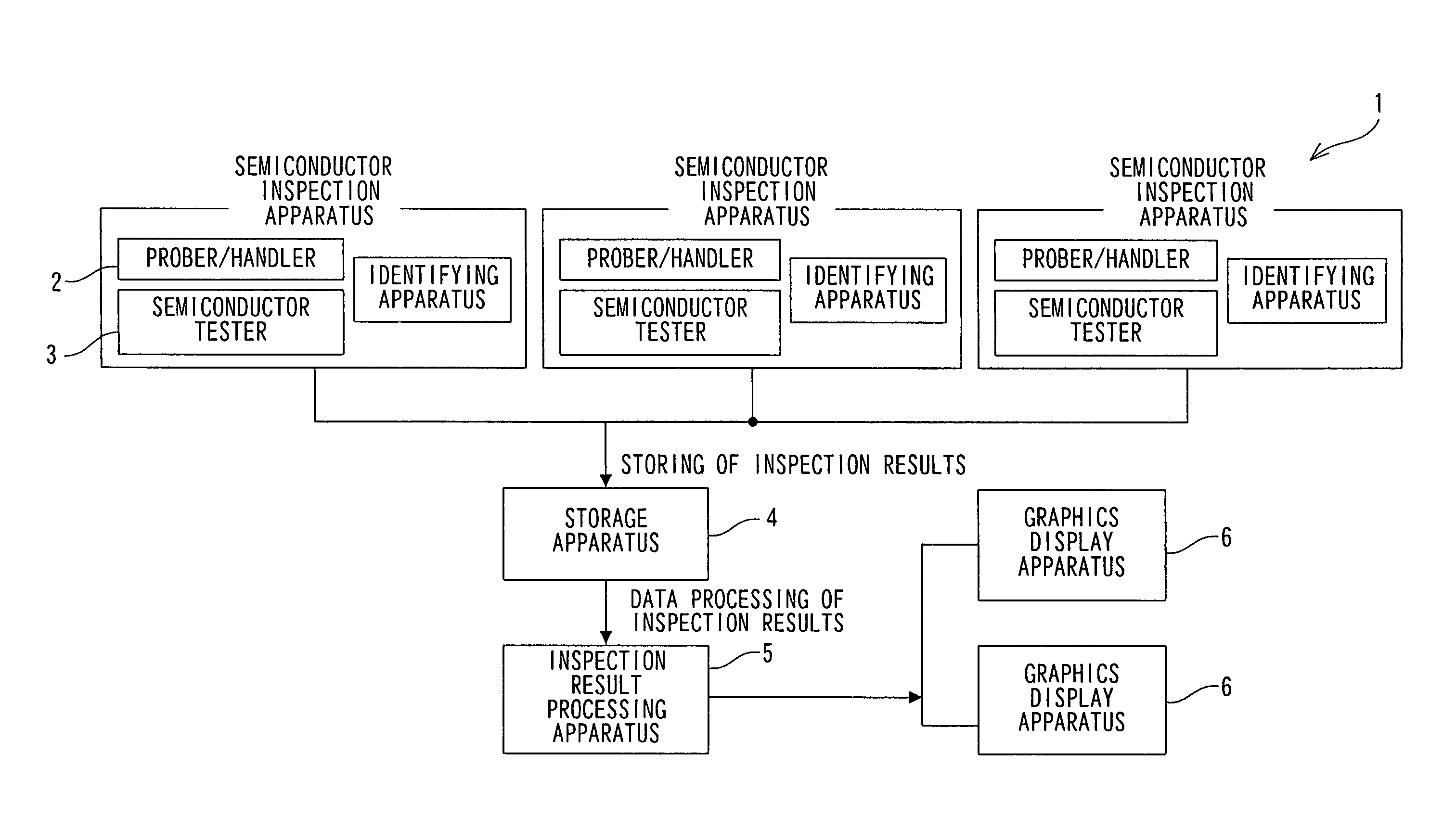
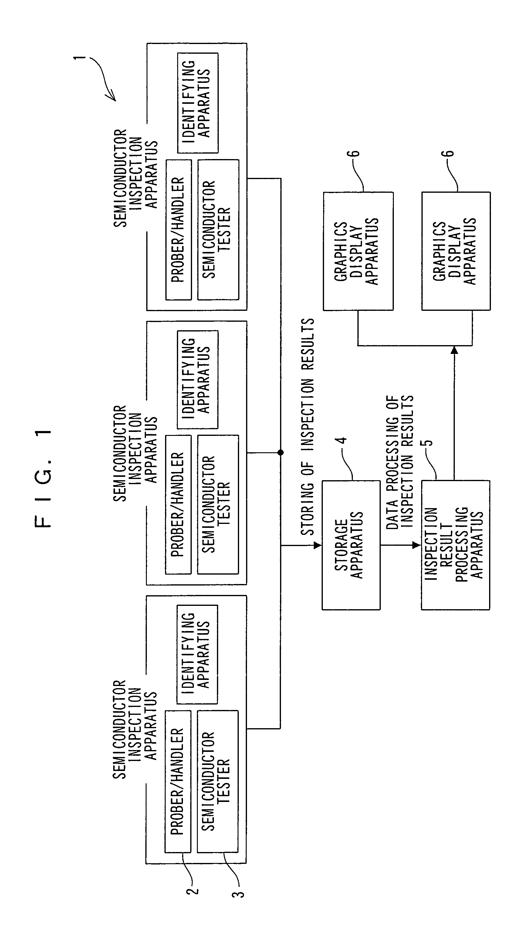
[0033]An embodiment of the present invention will be described below in accordance with the accompanying drawings. FIG. 1 is a schematic diagram showing the configuration of the present invention. A semiconductor inspection apparatus 1 comprises a so-called wafer prober or a handler 2. Generally a prober is used before a semiconductor wafer is split, and a handler is used after a semiconductor wafer is split (after packaging and sealing). A semiconductor tester 3 is a machine for inspecting electrical characteristics of a semiconductor product. Various kinds of semiconductor testers are available.

[0034]In order to use the semiconductor inspection apparatus 1 and the semiconductor tester 3 in the present invention, it is necessary to transmit inspection results on electrical characteristics to a host computer and the like via a communication line. The semiconductor tester 3 in recent years can transmit inspection results via a communication line in most cases.

[0035]The prober 2 which...


PUM

PropertyMeasurementUnit
electrical characteristicaaaaaaaaaa
shapeaaaaaaaaaa
electrical characteristicsaaaaaaaaaa

Abstract

An image of the shape of a semiconductor wafer is displayed on a display apparatus for displaying an inspection result of a semiconductor device, and a different color or pattern is displayed for each inspection result as display information indicating the inspection result of a semiconductor device in a region corresponding to the semiconductor device on the image of the semiconductor wafer.

Description

FIELD OF THE INVENTION[0001]The present invention relates an apparatus and method for inspecting a semiconductor device, particularly to a technique for displaying graphically and colorfully inspection results of semiconductor devices formed on a semiconductor wafer, as a visually recognizable semiconductor wafer map.BACKGROUND OF THE INVENTION[0002]Generally a number of semiconductor devices are simultaneously formed on a semiconductor wafer by, for example, a technique of precisely transferring photographs. Thereafter, the semiconductor wafer is cut along scribe lines and semiconductor devices formed on the semiconductor wafer are split as semiconductor chips.[0003]Conventional inspections conducted in a process of manufacturing the semiconductor device include, for example, inspections of electrical characteristics. Some inspections of electrical characteristics are conducted before a plurality of semiconductor devices formed on the semiconductor wafer are split into semiconducto...

Claims


Application Information

Patent Timeline
Patent Type & Authority Patents(United States)
IPC IPC(8): G01N37/00G06F19/00G01R31/28H01L21/00H01L21/66
CPCH01L21/67253H01L21/67288H01L21/67271
Inventor NISHIMURA, SATORU
Owner PANASONIC CORP
Why Eureka
Try Eureka