
Semiconductor device

a technology of semiconductor devices and interconnect wires, which is applied in the direction of semiconductor devices, semiconductor/solid-state device details, electrical apparatus, etc., can solve the problems of reducing the reliability of all fuse interconnect wires, affecting the overall quality of lsi chips, and increasing the laser beam energy

Inactive Publication Date: 2006-06-27
KK TOSHIBA
View PDF18 Cites 14 Cited by
  • Summary
  • Abstract
  • Description
  • Claims
  • Application Information

AI Technical Summary

Benefits of technology

[0018]According to an aspect of the present invention, there is provided a semiconductor device comprising: a substrate; a plurality of dielectric films formed on the substrate, laid one upon another; and a fuse interconnect-wire formed above the substrate and covered with a predetermined one of the dielectric films, and including a fuse main body which is to be blown to electrically disconnect the fuse interconnect-wire, which is smaller than a bottom of a fuse-blowing recess made in the predetermined dielectric film, which has a length more than the diameter of a fuse-blowing laser beam and which opposes the bottom of the fuse-blowing recess.
[0018]According to an aspect of the present invention, there is provided a semiconductor device comprising: a substrate; a plurality of dielectric films formed on the substrate, laid one upon another; and a fuse interconnect-wire formed above the substrate and covered with a predetermined one of the dielectric films, and including a fuse main body which is to be blown to electrically disconnect the fuse interconnect-wire, which is smaller than a bottom of a fuse-blowing recess made in the predetermined dielectric film, which has a length more than the diameter of a fuse-blowing laser beam and which opposes the bottom of the fuse-blowing recess.
[0019]According to another aspect of the present invention, there is provided a semiconductor device comprising: a plurality of dielectric films formed on a substrate, laid one upon another; and a fuse interconnect-wire which is formed above the substrate and covered with a predetermined one of the dielectric films, and which comprises a fuse lead and a fuse main body electrically connected to the fuse lead, the fuse main body lying below a bottom of a fuse-blowing recess made in the predetermined dielectric film and above the fuse lead, having a length more than the diameter of a fuse-blowing laser beam, and having both ends within an area opposite the bottom of the fuse-blowing recess, the both ends being spaced apart in the lengthwise direction of the fuse main body.
[0019]According to another aspect of the present invention, there is provided a semiconductor device comprising: a plurality of dielectric films formed on a substrate, laid one upon another; and a fuse interconnect-wire which is formed above the substrate and covered with a predetermined one of the dielectric films, and which comprises a fuse lead and a fuse main body electrically connected to the fuse lead, the fuse main body lying below a bottom of a fuse-blowing recess made in the predetermined dielectric film and above the fuse lead, having a length more than the diameter of a fuse-blowing laser beam, and having both ends within an area opposite the bottom of the fuse-blowing recess, the both ends being spaced apart in the lengthwise direction of the fuse main body.

Problems solved by technology

This may also cause the overall quality of the LSI chip to suffer.
Increasing the laser beam energy may damage a Cu fuse interconnect-wire adjacent to a target fuse interconnect-wire to be disconnected.
This may lower the reliability of all the fuse interconnect-wires 103.
As described above, increasing the thickness of the remaining film 104 results in restrictions on the arrangement of the Cu fuse interconnect-wires 103; that is, limitations are encountered in making the pitch of the interconnect-wires finer.
This reduces the rate at which chips are relieved through fuse blow, i.e., the manufacturing yield of LSI chips.
This may result in an increase in the process cost of LSIs.
That is, LSI chips become easy to suffer deterioration in quality.
This will make the fuse interconnect-wires 103 easy to be damaged by fuse blow as described above, lowering their reliability.

Method used


Image

  • Semiconductor device
  • Semiconductor device
  • Semiconductor device

Examples


first embodiment

[First Embodiment]

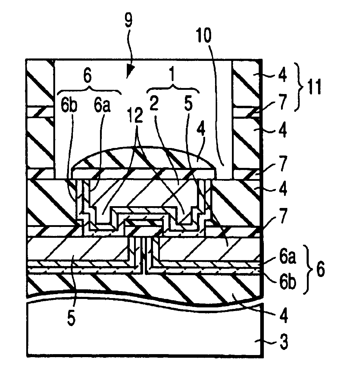
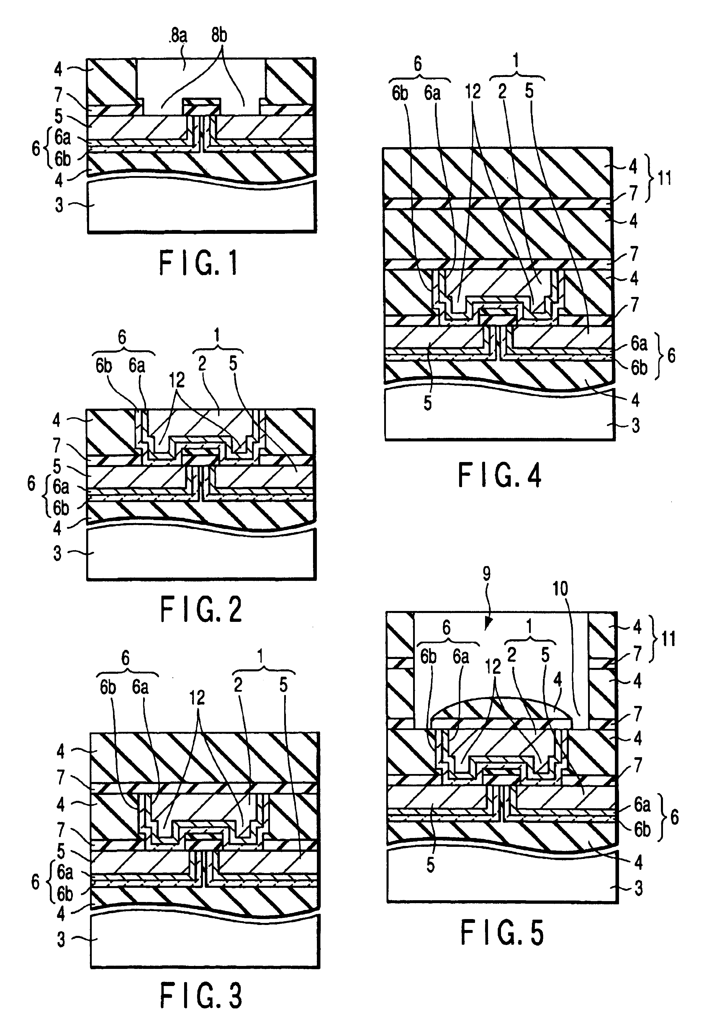
[0050]FIGS. 1 to 5 are sectional views of the LSI, explaining some steps of manufacturing the LSI as a semiconductor device according to the first embodiment. FIGS. 1 to 5 shows only one fuse interconnection-wire 1. Nonetheless, two or more fuse interconnection-wires may be provided. This holds true of the structures shown in FIGS. 8 to 12, which will be described later. The fuse interconnection-wire 1 is made of Cu and has a fuse main body 2 which is formed integral with a contact plug (via plug) 12. The contact plug 12 connects the main body 2 to a lead 5. Thus, the fuse main body 2 and the contact plug 12 have a so-called “dual damascene structure.”

[0051]First, as shown in FIG. 1, an Si substrate 3 has been formed with active devices (not shown) and multi-layered interconnect-wires (not shown) which make up various electronic circuits. The substrate 3 provided on top with the n-th layer (n is a positive integer) of inter-level dielectric film (ILD film) 4. The C...

second embodiment

[Second Embodiment]

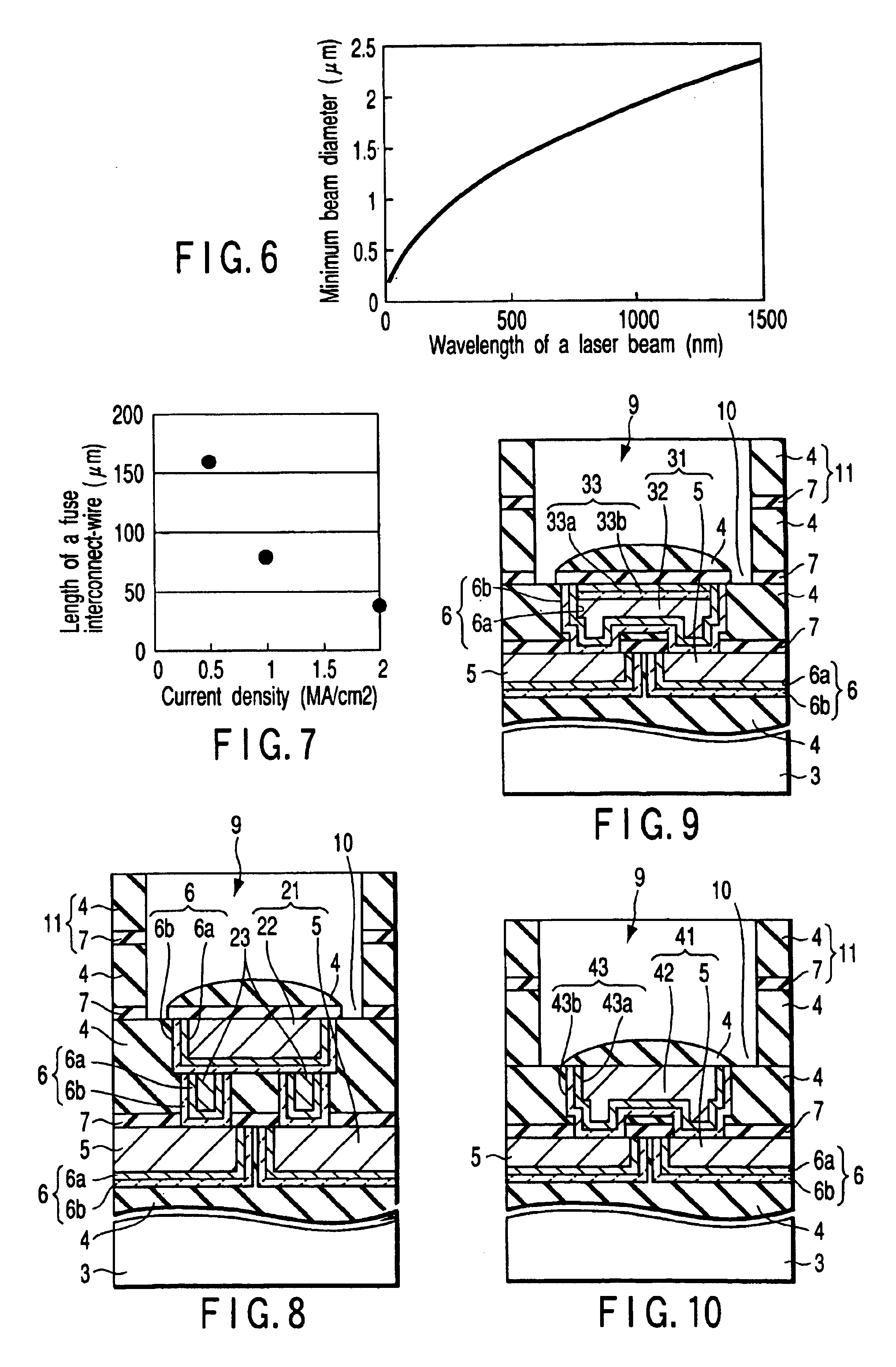
[0070]FIG. 8 is a sectional view of a semiconductor device according to the second embodiment, illustrating fuse interconnect-wires and the components provided near the wires. The components identical to those shown in FIGS. 1 to 5 are designated at the same reference numerals in FIG. 8 and will not be described in detail.

[0071]The fuse interconnect-wires 21 of the second embodiment are made of Cu. As shown in the FIG. 8, the fuse main body 22 of each fuse interconnect-wire 21 is not formed integral with the contact plug (via plug) 23; it is separated from the contact plugs (via plugs) 23 are formed separately. That is, the Cu fuse main body 22 has a so-called “single damascene structure.”

[0072]Up to the formation of the m-th layer of Cu diffusion barrier film 7, the process uses the same steps as with the first embodiment.

[0073]Next, a Cu fuse main body 22 of a single damascene structure is formed in the (n+1)-st layer of inter-level dielectric film 4 provided on...

third embodiment

[Third Embodiment]

[0077]FIG. 9 is a sectional view of a semiconductor device according to the third embodiment, depicting fuse interconnect-wires and the components provided near the wires. The components identical to those shown in FIGS. 1 to 5 are designated at the same reference numerals in FIG. 9 and will not be described in detail.

[0078]In this embodiment as well, a fuse interconnect-wire 31 is formed of Cu. The fuse main body 32 of the fuse interconnect-wire 31 is formed on top with a top barrier film 33 for preventing oxidation and diffusion of Cu.

[0079]Up to the formation of the Cu fuse main body 32, the process remains unchanged from that in the first embodiment. Thus, the fuse main body 32 of this embodiment is the dual damascene structure.

[0080]After the formation of the Cu fuse main body 32, its top is selectively recessed by means of wet etching or dry etching. After that, the top barrier film (top barrier metal film) 33 is formed on the recessed portion, which is the t...


PUM


Abstract

A semiconductor device comprising a substrate, a plurality of dielectric films formed on the substrate, laid one upon another, and a fuse interconnect-wire formed above the substrate and covered with a predetermined one of the dielectric films, and including a fuse main body which is to be blown to electrically disconnect the fuse interconnect-wire, which is smaller than a bottom of a fuse-blowing recess made in the predetermined dielectric film, which has a length not less than the diameter of a fuse-blowing laser beam and which opposes the bottom of the fuse-blowing recess.

Description

CROSS-REFERENCE TO RELATED APPLICATIONS[0001]This application is based upon and claims the benefit of priority from the prior Japanese Patent Application No. 2002-041974, filed on Feb. 19, 2002, the entire contents of which are incorporated herein by reference.BACKGROUND OF THE INVENTION[0002]1. Field of the Invention[0003]The present invention relates to the structure of interconnect-wires in a semiconductor device. More specifically, the invention relates to improvements in the interconnection pattern and structure of fuse interconnect-wires in an LSI chip.[0004]2. Description of the Related Art[0005]Semiconductor devices are generally known, which have a redundancy circuit for disabling defects components, if any. Most redundancy circuits have fuse interconnect-wires. The fuse interconnect-wires may be blown when applied with a laser beam, to disconnect the defective components from the normally functioning components.[0006]Here, the fuse interconnect-wires and some associated co...

Claims


Application Information

Patent Timeline
Patent Type & Authority Patents(United States)
IPC IPC(8): H01L29/00H01L23/525H01L23/532
CPCH01L23/5258H01L23/53223H01L23/53238H01L2924/12044H01L2924/0002H01L2924/00H01L21/82
Inventor HATANO, MASAAKIIKEGAMI, HIROSHIUSUI, TAKAMASAMATSUO, MIE
Owner KK TOSHIBA
Learn More