Plasma display panel device and its drive method

a technology of plasma display panel and drive method, which is applied in the direction of instruments, gas discharge vessels/containers, and address electrodes. it can solve the problems of significant power consumption challenge to drive the pdp with a small amount of power consumption, and large power consumption of wide transparent electrodes

Inactive Publication Date: 2006-06-27
PANASONIC CORP
View PDF13 Cites 11 Cited by
  • Summary
  • Abstract
  • Description
  • Claims
  • Application Information

AI Technical Summary

Benefits of technology

[0116]FIG. 7 is an example of a V-Q Lissajous's figure. In this figure, the loop “a” schematically represents a case where the PDP is driven using a sustain pulse having a simple rectangular waveform, and the loop “b” schematically represents a case where the PDP is driven using a sustain pulse having the above-described staircase waveform.
[0117]The V-Q Lissajous's figures show how the quantity of electric charge Q changes forming a loop. There is a relationship that the area of a loop in the V-Q Lissajous's figures is approximately proportionate to an amount of power consumed in discharge.
[0118]The quantity of electric charge Q accumulated in the discharge cells can be measured by connecting the PDP with a wall charge amount measuring apparatus that uses the same principle as the Sawyer-Tower circuit that is used for evaluating ferro electric characteristics or the like.
[0119]The loops “a” and “b” are both V-Q Lissajous's figures and parallelograms, but the loop “b” is distorted and narrower than the loop “a”. Also, the loop “b” has arc-shaped sides.
[0120]The narrower the parallelogram is, the smaller the loop area is. This indicates that when the parallelogram is narrow, while the amount of charge moving in the discharge cells does not change, and the amount of emitted light does not change, the amount of power consumption in the PDP is small.
[0121]As described above, when the staircase waveform is used, the loop “b” becomes narrower. It is considered that this is because the second period, in which the high-level voltage V2 is applied, follows the first period. Also, another reason why the loop reduces in the direction of Q (vertical direction in the drawings) is that the third period, in which a voltage lower than the discharge start voltage is applied, follows the second period.

Problems solved by technology

In such a PDP, it is a significant challenge to drive the PDP with a small amount of power consumption.
The problem of the power consumption becomes more significant when wide transparent electrodes are used to improve the luminance in image display.
This is because the wide transparent electrodes consume a lot of power.
Accordingly, in such a case, it is difficult to control the gray scale.
This is another problem.
Too short a time period of the write pulse causes a write defect, degrading the image quality.
When a simple rectangular wave is used as the sustain pulse, if the data pulse width is set to approximately 2 μs or shorter, the discharge probability at the sustain discharge decreases, and this is apt to cause the image quality degradation.

Method used


Image

  • Plasma display panel device and its drive method
  • Plasma display panel device and its drive method
  • Plasma display panel device and its drive method

Examples


embodiment 1

[0056]A plasma display apparatus (PDP display apparatus) includes, for example, a PDP and a driving circuit.

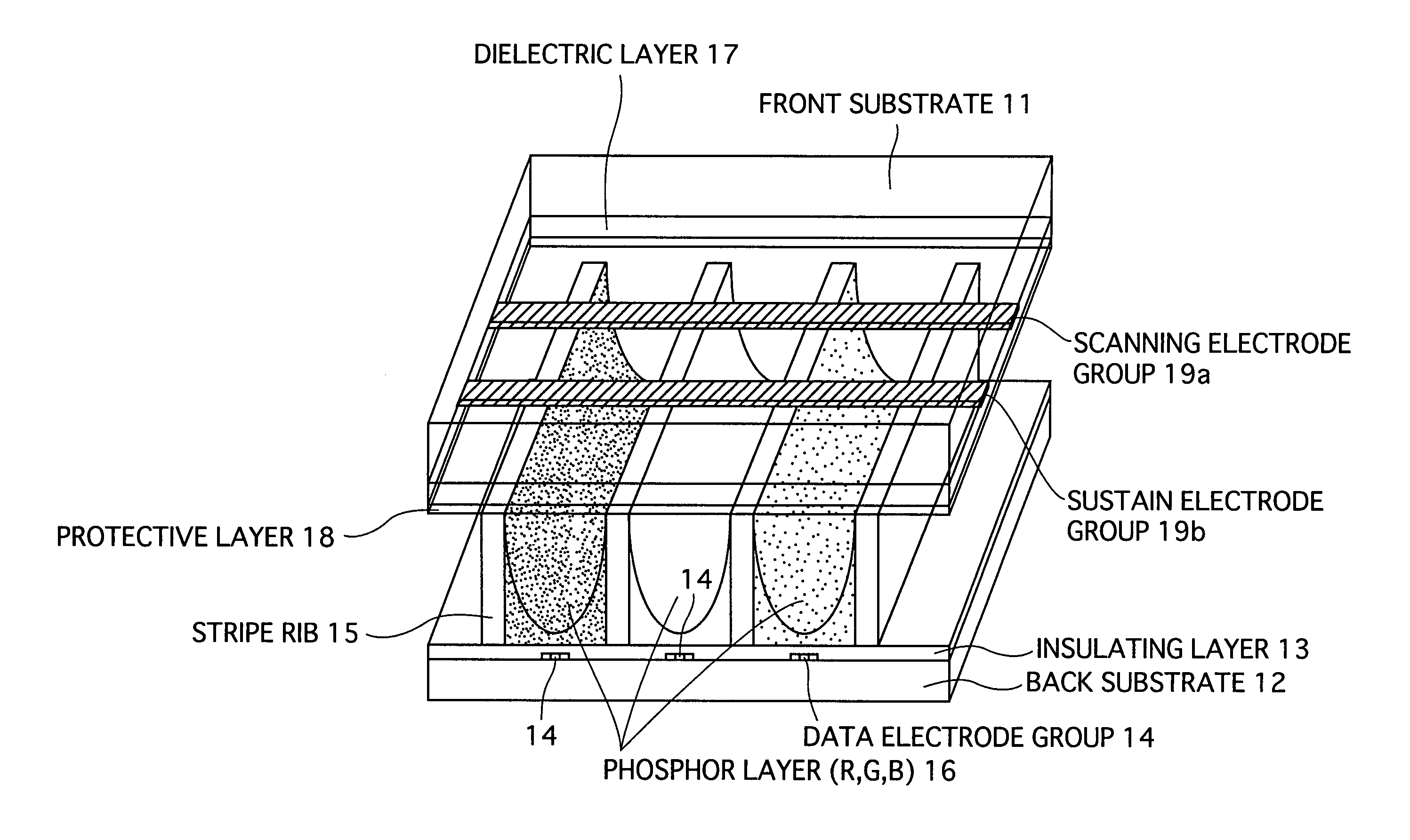
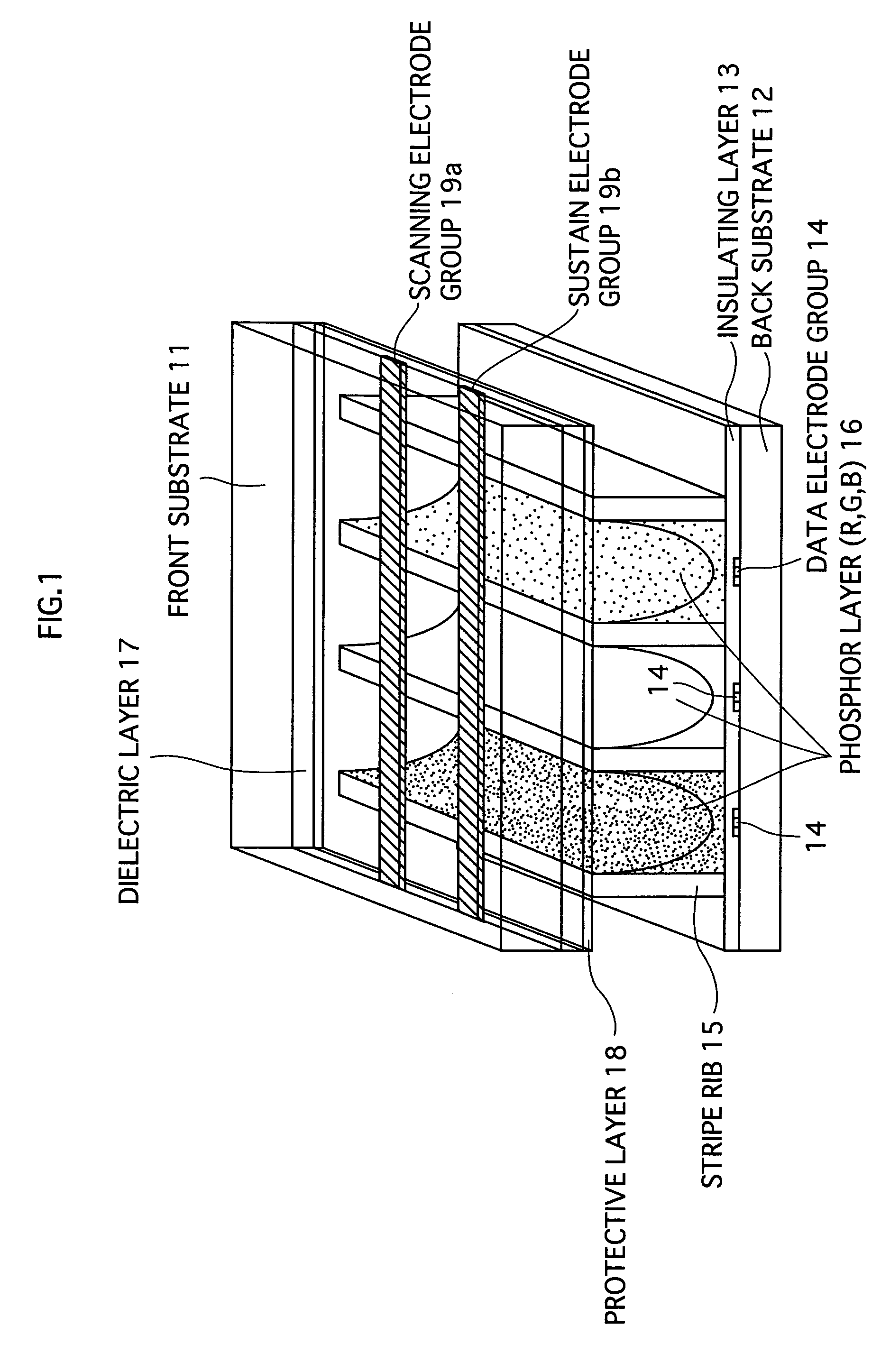
[0057]FIG. 1 shows the construction of the PDP in the present embodiment.

[0058]In this PDP, a front substrate 11 and a back substrate 12 are placed in parallel so as to face each other with a space in between. The edges of the substrates are then sealed.

[0059]Scanning electrode group 19a and sustain electrode group 19b are formed in parallel strips on the inward-facing surface of the front substrate 11, forming a plurality of pairs of a scanning electrode and a sustain electrode. The electrode groups 19a and 19b are covered by a dielectric layer 17 composed of lead glass or similar. The surface of the dielectric layer 17 is then covered with a protective layer 18 of magnesium oxide (MgO). A data electrode group 14 is formed in parallel strips so as to be perpendicular to the scanning electrode group 19a, on the inward-facing surface of the back substrate 12. The data electrode...

embodiment 2

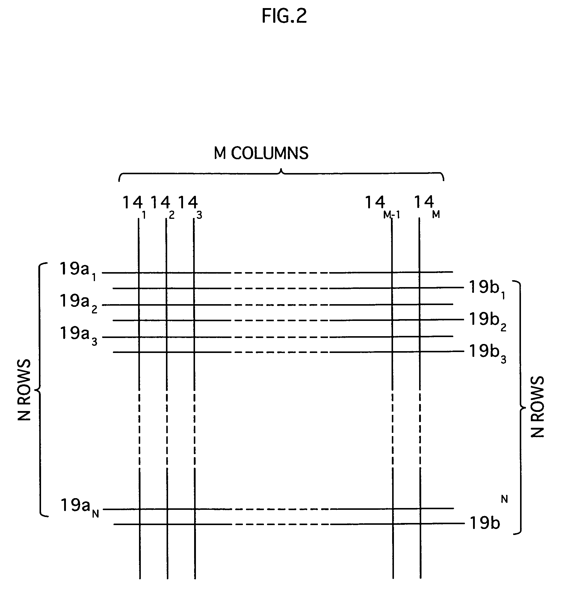
[0151]FIG. 12 is a schematic illustration of an electrode pattern in the present embodiment.

[0152]The driving waveform applied to each electrode by the driving circuit in the present embodiment is the same as Embodiment 1. In the present embodiment, the sustain pulse has the two-step rise / fall staircase waveform shown in FIGS. 5A, 5B, and 6. The PDP in the present embodiment has the same construction as that in Embodiment 1, except for the electrode construction as the following description will show.

[0153]In Embodiment 1, each of the electrode groups 19a and 19b has a laminated structure of two layers: a layer of transparent electrodes; and a layer of metal electrodes. Different from this, Embodiment 2 has a split electrode (FE electrode) structure in which each of the electrode groups 19a and 19b is divided into thin line electrodes.

[0154]As shown in FIG. 12, the scanning electrode 19a is composed of three line electrodes 191a–193a that are parallel to each other. Similarly, the s...

example 1

[0213]Example 1 is a PDP with the split electrode structure described in Embodiment 2, and is set as follows: the pixel pitch P=1.08 mm; the main discharge gap G=80 μm; electrode width (L1, L2, L3)=40 μm; and the first electrode gap S1=the second electrode gap S2=70 μm.

[0214]Also, in Example 1, a sustain pulse having two rise steps is used when the PDP is driven.

[0215]FIG. 17A shows the waveform of the sustain pulse and the waveform of the discharge current that is generated when the sustain pulse is applied. As shown in FIG. 17A, the rise start point t2 of the second step precedes the point t5 at which the discharge current is at the maximum. FIG. 17B shows the waveforms of the sustain pulse and the discharge current of a comparative example which is a PDP having the same construction as Example 1 but is different in that the sustain pulse has a simple rectangular waveform.

[0216]As shown in FIG. 17B: the discharge current waveform has a single peak; the discharge light emission end...


PUM


Abstract

It is the object of the invention to provide a PDP apparatus and a driving method that can apply pulses at high speeds and can display high-definition, high-quality images by allowing discharge cells to emit light with high luminance and high efficiency.To achieve the object, the pulse has (i) a first waveform portion where a first voltage, an absolute value of which is no smaller than a discharge start voltage, is applied and (ii) a second waveform portion where a second voltage, an absolute value of which is greater than the absolute value of the first voltage, is applied, the second waveform portion following the first waveform portion, and the second waveform portion starts before a discharge delay time elapses from a start of the first waveform portion.Also to achieve the object, in a PDP having an electrode structure in which each electrode is divided into a plurality of line electrodes, the applied pulse has (i) a first waveform portion where a first voltage, an absolute value of which is no smaller than a discharge start voltage, is applied and (ii) a second waveform portion where a second voltage, an absolute value of which is greater than the absolute value of the first voltage, is applied, the second waveform portion following the first waveform portion.

Description

TECHNICAL FIELD[0001]The present invention relates to a plasma display panel apparatus that is used as the display screen for computers, televisions and the like, and a driving method thereof, and in particular to an AC plasma display panel.BACKGROUND ART[0002]Recently, plasma display panels (hereafter referred to as PDPs) have become the focus of attention for their ability to realize a large, slim and lightweight display apparatus for use in computers, televisions and the like.[0003]PDPs can be broadly divided into two types: direct current (DC) and alternating current (AC). Of these, AC PDPs are at present the dominant type.[0004]In a typical AC PDP, a front substrate and a back substrate are placed in parallel so as to face each other. A scanning electrode group and a sustain electrode group are formed in parallel strips on the inward-facing surface of the front substrate. The electrode groups are covered by a dielectric layer. A data electrode group is formed in parallel strips...

Claims


Application Information

Patent Timeline
Patent Type & Authority Patents(United States)
IPC IPC(8): G09G3/28G09G3/288G09G3/291G09G3/293G09G3/294G09G3/296G09G3/298H01J11/12H01J11/14H01J11/22H01J11/24H01J11/26H01J11/32H01J11/34
CPCG09G3/2942G09G3/2965G09G3/2986G09G3/2983G09G3/2022G09G2330/021G09G2320/0238G09G2320/0252G09G3/296
Inventor NAGAO, NOBUAKIANDO, TORUNISHIMURA, MASAKIHIGASHINO, HIDETAKATAKADA, YUUSUKE
Owner PANASONIC CORP
Why Eureka
Try Eureka