
Electrostatic discharge protection device

Inactive Publication Date: 2006-07-11
WINBOND ELECTRONICS CORP
View PDF2 Cites 1 Cited by
  • Summary
  • Abstract
  • Description
  • Claims
  • Application Information

AI Technical Summary

Benefits of technology

The present invention provides an electrostatic discharge protection device with effective long gate fingers that eliminate the drawbacks of prior art devices. The device includes a first isolation region, an active region, a second isolation region, and a first gate element with first and second ends. The device also includes a drain region, a source region, and drain and source contacts. The invention also includes a semiconductor device with first and second isolation regions and a first conductive element with first and second ends. The invention achieves an equivalent long gate finger enabling the cascading effect.

Problems solved by technology

This potentially prevents other gate fingers from turning on.

Method used


Image

  • Electrostatic discharge protection device
  • Electrostatic discharge protection device
  • Electrostatic discharge protection device

Examples


first embodiment

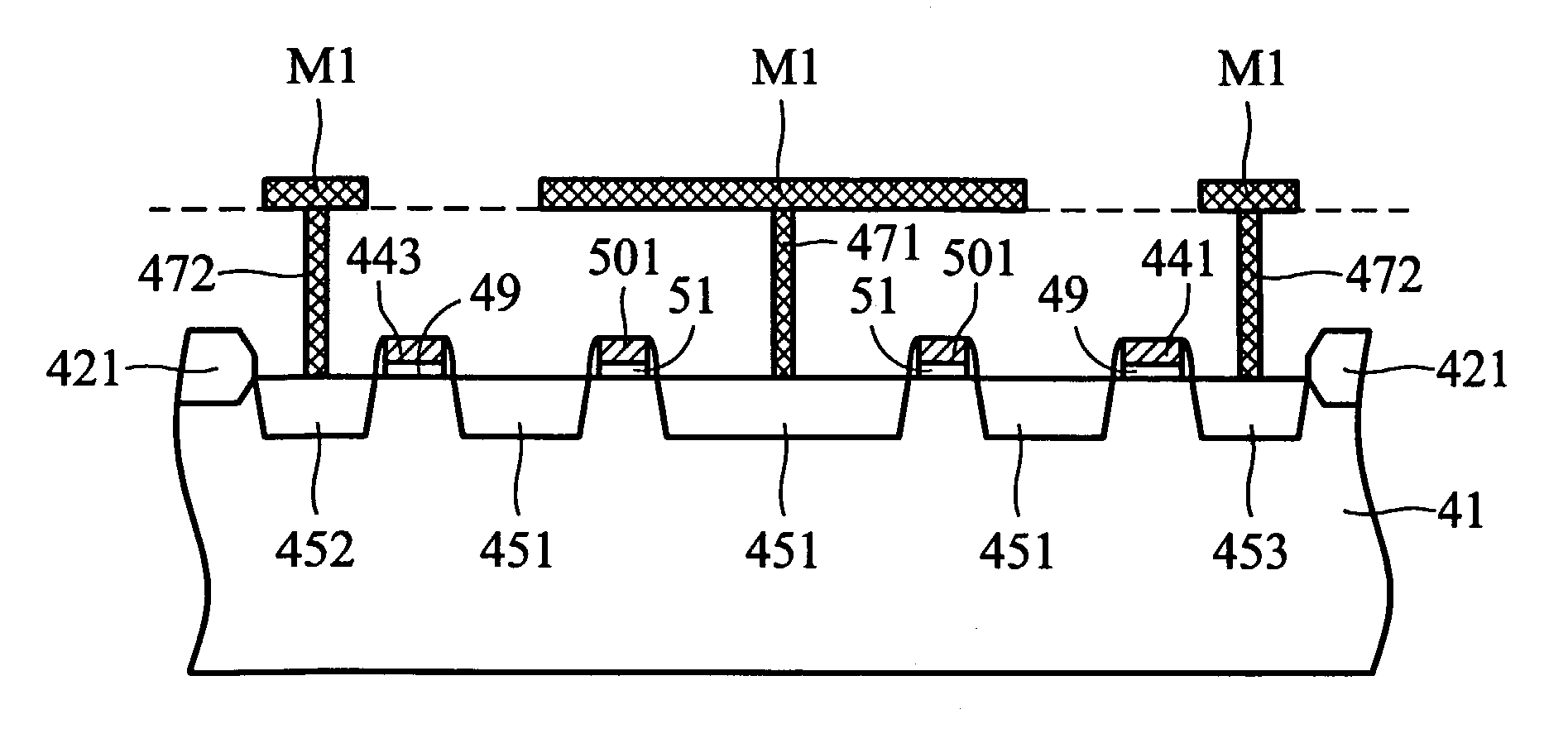
[0027]FIGS. 4A, 4B, 4C and 4D are diagrams showing an ESD protection device according to the invention. FIGS. 4B, 4C and 4D show cross sections of FIG. 4A along line AA′, BB′ and CC′ respectively. The electrostatic discharge protection device is formed on a substrate 41 and comprises an isolation region 421 formed over the substrate 41, an active region 43 formed over the substrate 41 and enclosed by the isolation region 421, another isolation region 422 formed on the substrate 41 and substantially surrounded by the active region 43, gates (conductive layer) 441, 442 and 443 formed in the active region 43, a drain region 451 formed in the active region 43 at one side of the gate 441, a source region 452 formed in the active region 43 at the other side of the gate 441, drain contacts 471 for electrically coupling the drain region 451 to a node 461, source contacts 472 for electrically coupling the source region 452 to a node 462. The gate 441 has one end extending over (overlapping)t...

second embodiment

[0029]FIGS. 5A, 5B and 5C are diagrams showing an ESD protection device according to the invention. FIGS. 5B and 5C show cross sections of FIG. 5A along line XX′ and YY′ respectively. The ESD protection devices shown in FIGS. 4A˜4D and 5A˜5C are similar except that there are islands 50 distributed in and surrounded by the drain region 451 in FIGS. 5A˜5C. For clarity, no reiteration is made to the same elements in FIGS. 4A˜4D and FIGS. 5A˜5C. The formation of the islands 50 is disclosed in U.S. Pat. No. 5,721,439.

[0030]The islands 50 are arranged in an array comprising at least one island 50 or multiple rows of the islands 50 which are distributed in the drain region 451 between the drain contacts 471, and the gates 441˜443 or the isolation region 422. The islands 50 may be poly-silicon elements 501 over an oxide layer. 51 simultaneously formed by the same process as the gate 441. The drain contacts 471 also form an array. The gates 441 and 442, and isolation region 422 form a first ...

third embodiment

[0031]FIGS. 6A, 6B and 6C are diagrams showing an ESD protection device according to the invention. FIGS. 6B and 6C show cross sections of FIG. 6A along line DD′ and EE′ respectively. The ESD protection devices shown in FIGS. 5A˜5C and 6A˜6C are similar except that the islands 50 are formed by field oxide layers 502 in FIGS. 6A˜6C. The islands 50 are preferably formed by the same construction as the surrounding isolation region 421 for the transistor. The isolation region 421 may be formed by STI or LOCOS process.


PUM


Abstract

An electrostatic discharge protection device formed on a substrate. The electrostatic discharge protection device includes a first isolation region formed over the substrate, an active region formed over the substrate and enclosed by the first isolation region, a second isolation region formed on the substrate and substantially surrounded by the active region, a first gate element formed in the active region, the first gate element having a first end extending over the first isolation region and a second end extending over the second isolation region, a drain region formed in the active region at a first side of the first gate element, a source region formed in the active region at a second side of the first gate element, a drain contact for electrically coupling the drain region to a first node, and a source contact for electrically coupling the source region to a second node.

Description

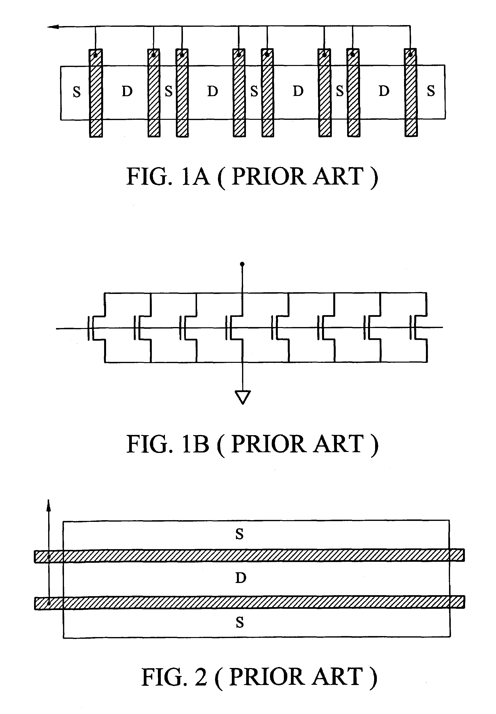
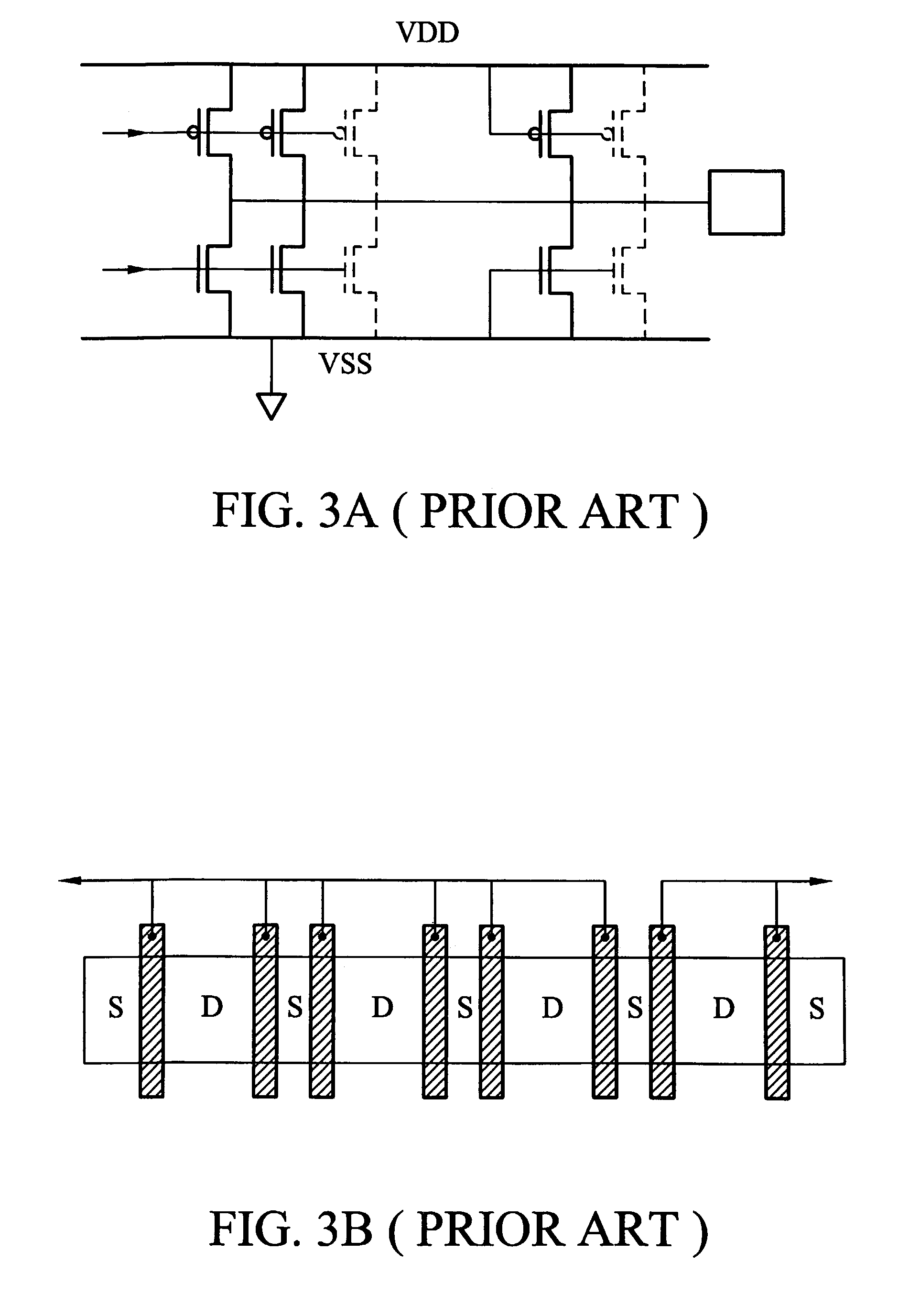
[0001]Pursuant to 35 U.S.C. § 119(a)–(d), this application claims priority from Taiwanese application no. 091106186, filed on Mar. 28, 2002.BACKGROUND OF THE INVENTION[0002]1. Field of the Invention[0003]The present invention relates to an electrostatic discharge (ESD) protection device and particularly to an ESD protection device with improved performance.[0004]2. Description of the Prior Art[0005]An NMOSFET is a very effective ESD protection device. In one application, with the gate connected to a gate-driving signal, the NMOSFET is used as the pull down device of a CMOS buffer to drive an output voltage. In a second application, with the gate electrically connected to the ground, the NMOSFET is used to protect an input pin or power bus during an ESD event.[0006]In a PS mode ESD event, with a positive ESD transient voltage applied to an IC pin while a VSS power pin is at ground potential, the protection of an NMOSFET heavily depends on the snap-back mechanism for conducting large ...

Claims


Application Information

Patent Timeline
Patent Type & Authority Patents(United States)
IPC IPC(8): H01L23/62H01L27/02H02H9/00
CPCH01L27/027H01L2924/0002H01L2924/00
Inventor LIN, SHI-TRONCHEN, WEI-FAN
Owner WINBOND ELECTRONICS CORP
Learn More