Tracking switchmode power converter for telephony interface circuit
a technology of telephony interface circuit and switchmode power converter, which is applied in the direction of electrical equipment, substation equipment, interconnection arrangements, etc., can solve the problems of waste of power and power for a short line length application, and achieve the effect of removing the effect of voltage drop through either diode and reducing the loading on the tip and ring
- Summary
- Abstract
- Description
- Claims
- Application Information
AI Technical Summary
Benefits of technology
Problems solved by technology
Method used
Image
Examples
first embodiment
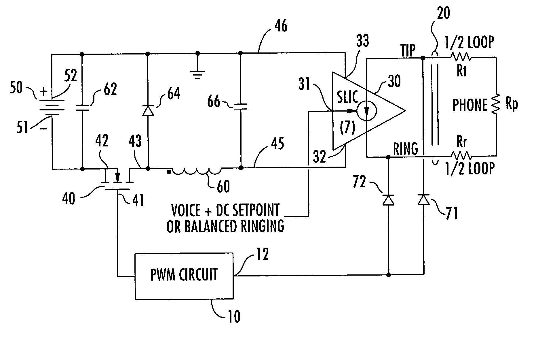
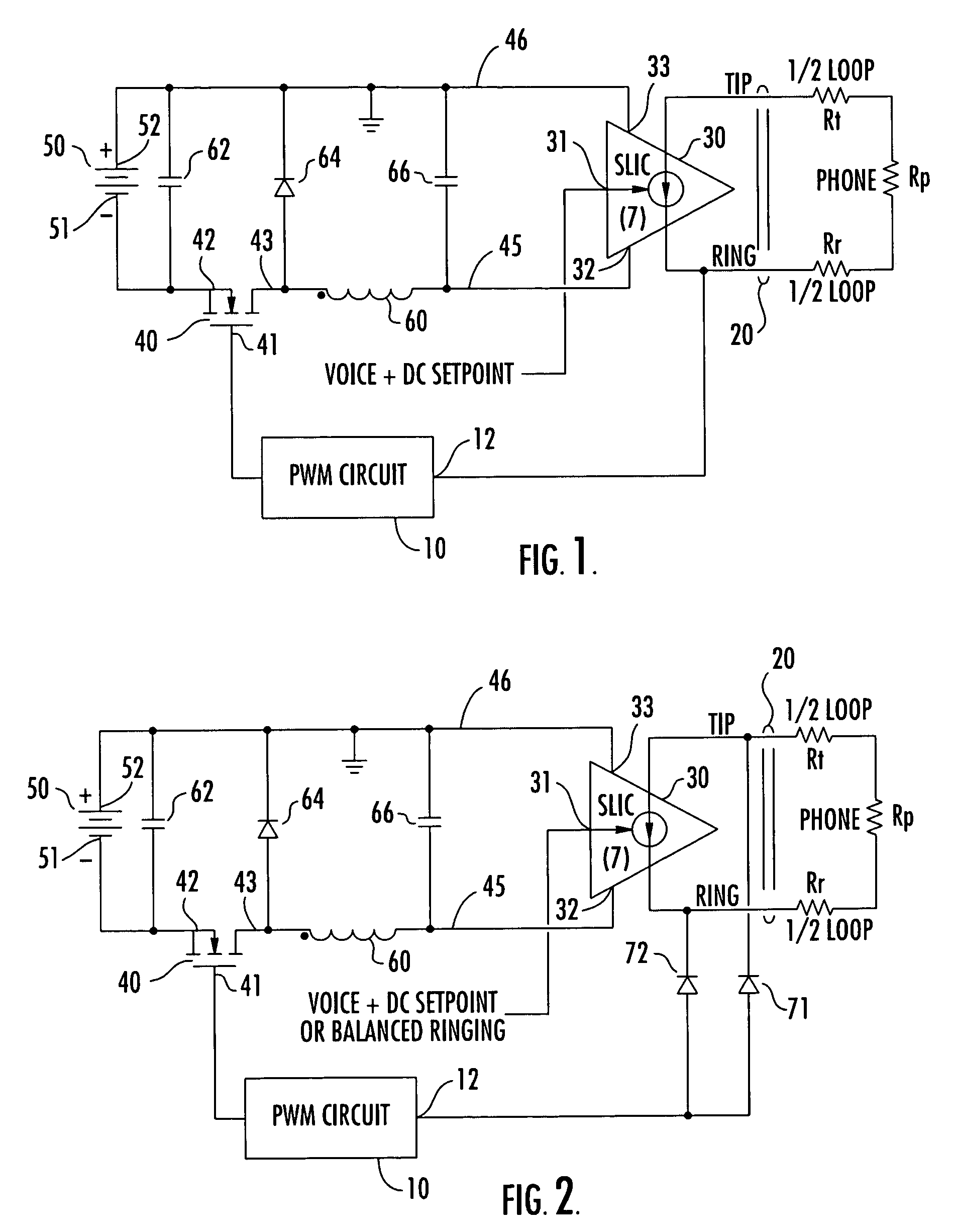
[0011]a switchmode power converter of the present invention is diagrammatically illustrated in FIG. 1 as comprising a pulse width modulator (PWM) circuit 10 having a sense input 12, which is coupled to monitor or sense the line voltage of one (e.g., Ring (R) of a tip / ring (T / R) loop pair 20, that are driven by a SLIC 30. The overall line resistance of the loop 20 is shown schematically by tip and ring resistances Rt and Rr, respectively, which form a closed loop circuit path with the resistance Rp of a phone terminating the loop.
[0012]SLIC 30 has a signalling input terminal 31 coupled to receive both signals and a prescribed DC loop current set point. The PWM circuit 10 is operative to generate a high frequency modulation waveform that is coupled to the control input (gate) 41 of an electronic switch, shown as a MOSFET 40, which is coupled in circuit with the DC power supply for the SLIC. PWM circuit 10 and MOSFET 40 form a switchmode power converter that is operative to actively mo...
second embodiment
[0016]FIG. 2 shows a diagrammatic illustration of a switchmode power converter of the present invention, in which the embodiment of FIG. 1 is modified to provide power supply tracking during balanced ringing. During a balanced ringing condition (e.g., at 20 Hz, as a non-limiting example), the SLIC will alternately drive the tip and ring portions of the loop 20 between the power rail (−V50) and ground, with tip and ring being 180° out of phase. This imposes a (20 Hz) ringing waveform on the line that has twice the peak-to-peak voltage of the power supply 50.
[0017]Since the voltage transition on tip or ring is generally controlled by the SLIC 30 to minimize ramp time, it would be beneficial for the power supply to track the output as its slews up and down (between its opposite polarity supply rail extremes). As shown in FIG. 2, this is accomplished by controlling the operation of the PWM circuit 10 in accordance with the greater magnitude of tip and ring. In particular, the sense inpu...
PUM
 Abstract
Description
Claims
Application Information


