Semiconductor pressure sensor
a technology of semiconductor devices and pressure sensors, applied in semiconductor devices, instruments, measurement devices, etc., can solve problems such as preventing correct pressure signals, and achieve the effect of improving endurance against pressure medium and small siz
- Summary
- Abstract
- Description
- Claims
- Application Information
AI Technical Summary
Benefits of technology
Problems solved by technology
Method used
Image
Examples
first embodiment
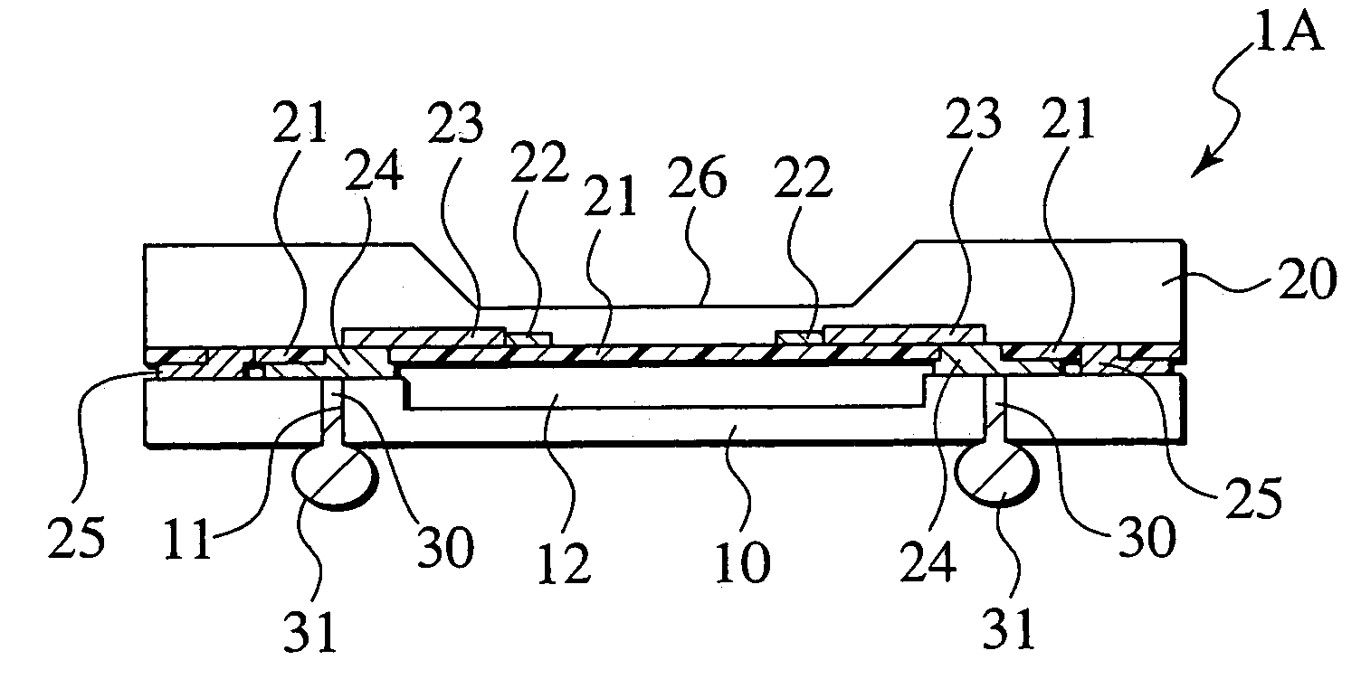
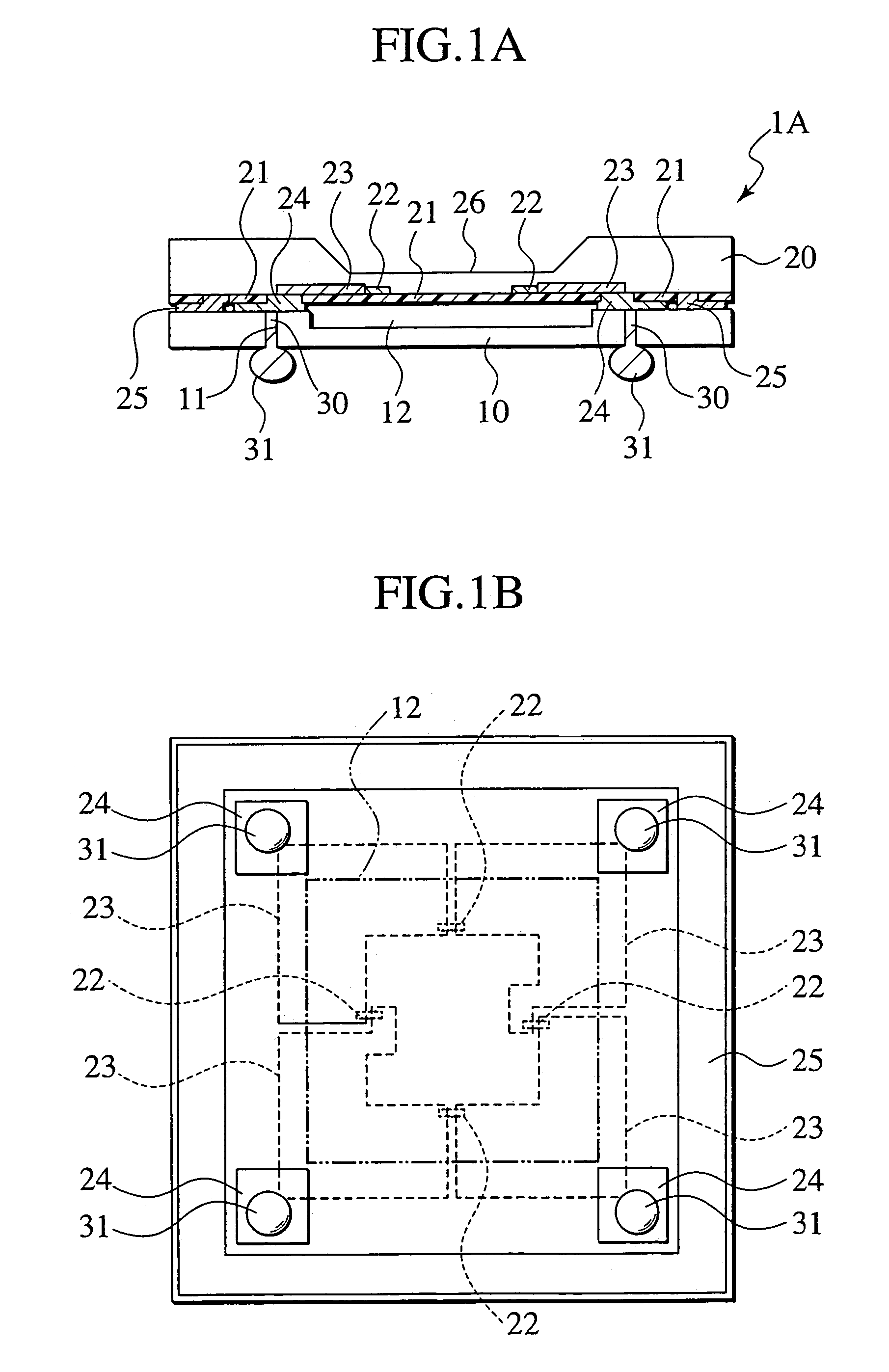
[0033]As illustrated in FIGS. 1A and 1B, this semiconductor pressure sensor 1A includes a glass support 10, a silicon chip 20 and through-hole interconnections 30.
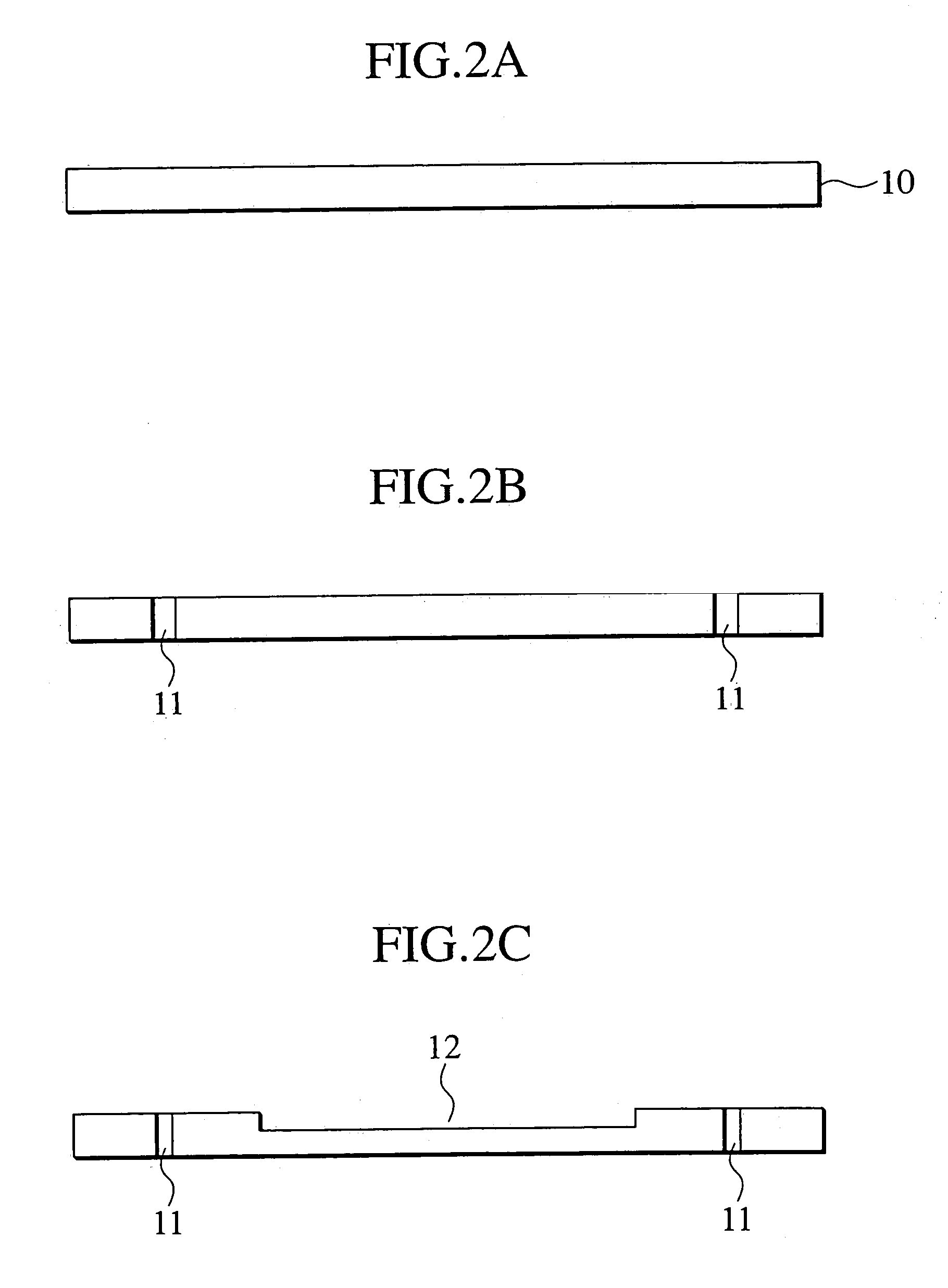
[0034]The glass support 10 has through-holes 11 formed in the four corners. The glass support 10 has a recess 12 formed in the central portion.
[0035]The silicon chip 20 includes four piezo-resistive elements 22 and four high-concentration lead layers 23 as a sensor circuit, each of which is formed on the bottom surface (the lower surface as shown in FIG. 1). The piezo-resistive elements 22 and the high-concentration lead layers 23 are interposed between the insulation-film 21 and the bottom surface. The four piezo-resistive elements 22 are connected in series by the four high-concentration lead layers 23, forming a bridge circuit. A respective one of lead layers 23 is connected to a corresponding one of metal pads 24 which outputs the signals from the piezo-resistive elements 22 to an external circuit. The metal pads 24 ar...
second embodiment
[0060]The following describes a second exemplary embodiment of the invention. Like reference numbers indicate elements similar to those described in the first exemplary embodiment, and thereby redundant explanation is not repeated.
[0061]In the case of a semiconductor pressure sensor 1B, a sealing metal 25 is formed inside of a metal pad 24 as shown in FIG. 11A and FIG. 11B. When the glass support 10 is anodic bonded to the silicon chip 20, the sealing metal 25 is required to electrically connect with a silicon substrate. For this reason, the sealing metal 25 is joined to the silicon substrate with joints 40 where no high-concentration lead parts 23 are formed.
[0062]It is possible that joints 40 have recesses lower than other locations where an insulation-film 21 is removed. Accordingly, it is desirable to form a thin insulation-film 21 for secure hermeticity, even if a recess is produced during bonding. In either joining method, attention should be paid to recesses of joints for sec...
third embodiment
[0064]The following describes a third exemplary embodiment of the invention. Like reference numbers indicate elements similar to those described in the first exemplary embodiment, and thereby redundant explanation is not repeated.
[0065]A semiconductor pressure sensor 1C of the third exemplary embodiment is different from the pressure sensor 1A of the first exemplary embodiment in that a silicon chip 20 has through-holes 27 therethrough as shown in FIG. 12.
[0066]The manufacturing method of this pressure sensor 1C will be described with reference to FIGS. 13A to 13D.
[0067]A glass support 10A is prepared without through-holes 11. Next, a silicon wafer is prepared, with silicon chip 20 formed with sensor circuit of FIG. 3A, as the manufacturing process of the first embodiment. As illustrated in FIG. 13A, the silicon chip 20A has through-holes 27 therethrough from the rear surface (i.e., the surface with no sensor circuit). A DRIE method such as the ICP-RIE method is employed for the for...
PUM
 Abstract
Description
Claims
Application Information


