
Optical writing head such as organic EL array exposure head, method of manufacturing the same, and image forming apparatus using the same

an exposure head and optical technology, applied in the field of optical writing heads, can solve the problems of condensing light-emitting parts, affecting the quality of the image, and requiring a long optical path length, so as to achieve the effect of reducing the number of exposure heads

Inactive Publication Date: 2006-07-25
SEIKO EPSON CORP
View PDF22 Cites 27 Cited by
  • Summary
  • Abstract
  • Description
  • Claims
  • Application Information

AI Technical Summary

Benefits of technology

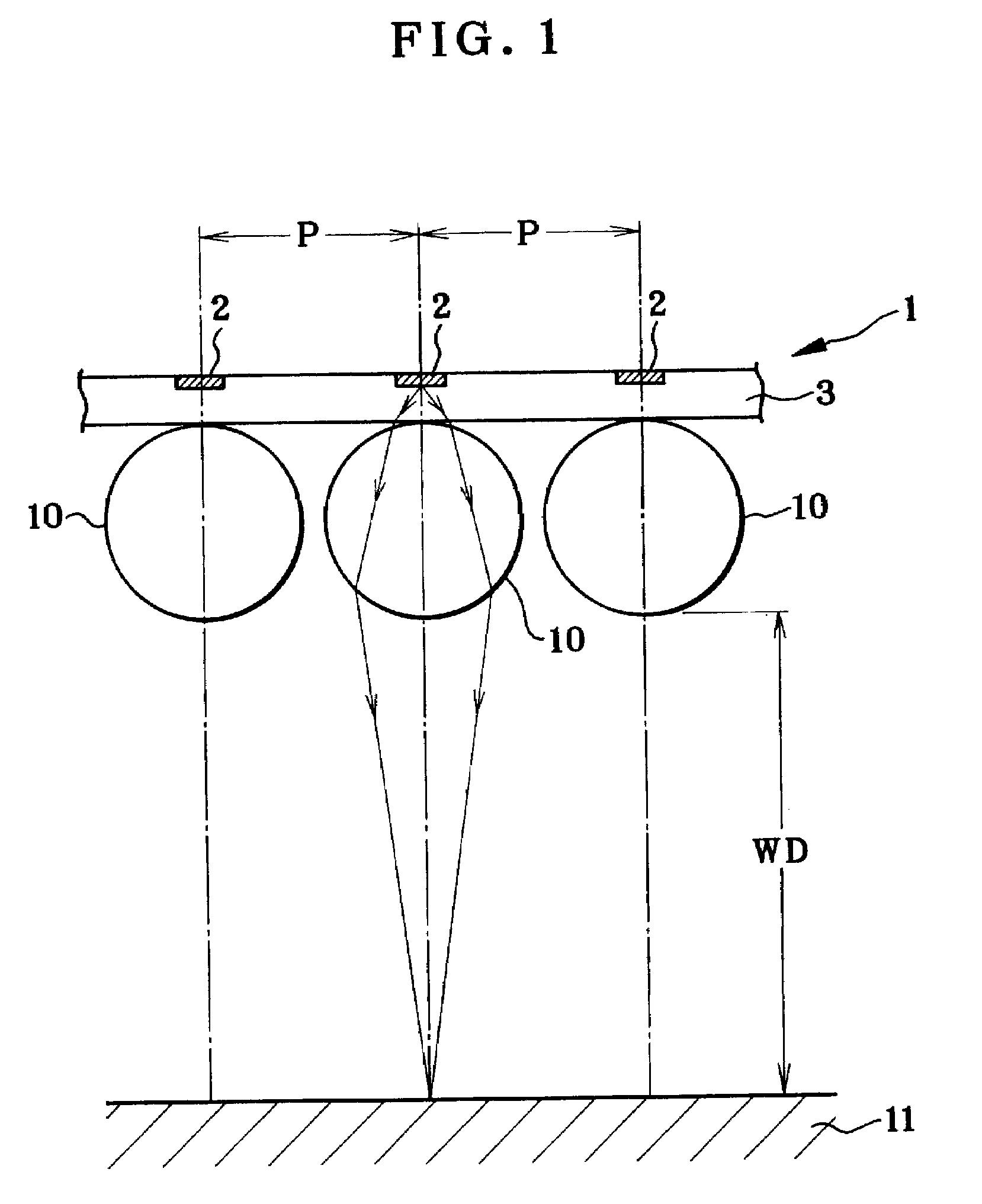
[0015]The first object is achieved by providing an optical writing head for projecting fluxes of modulated light from light-emitting parts of a light-emitting element array or fluxes of modulated light transmitted through shutter parts of an optical shutter element array onto an image carrier to form a predetermined pattern on the image carrier, wherein the optical writing head is characterized by comprising ball lenses which are arranged such that the alignment of the ball lenses corresponds to the alignment of the light-emitting parts of the light-emitting element array or the shutter parts of the optical shutter element array.
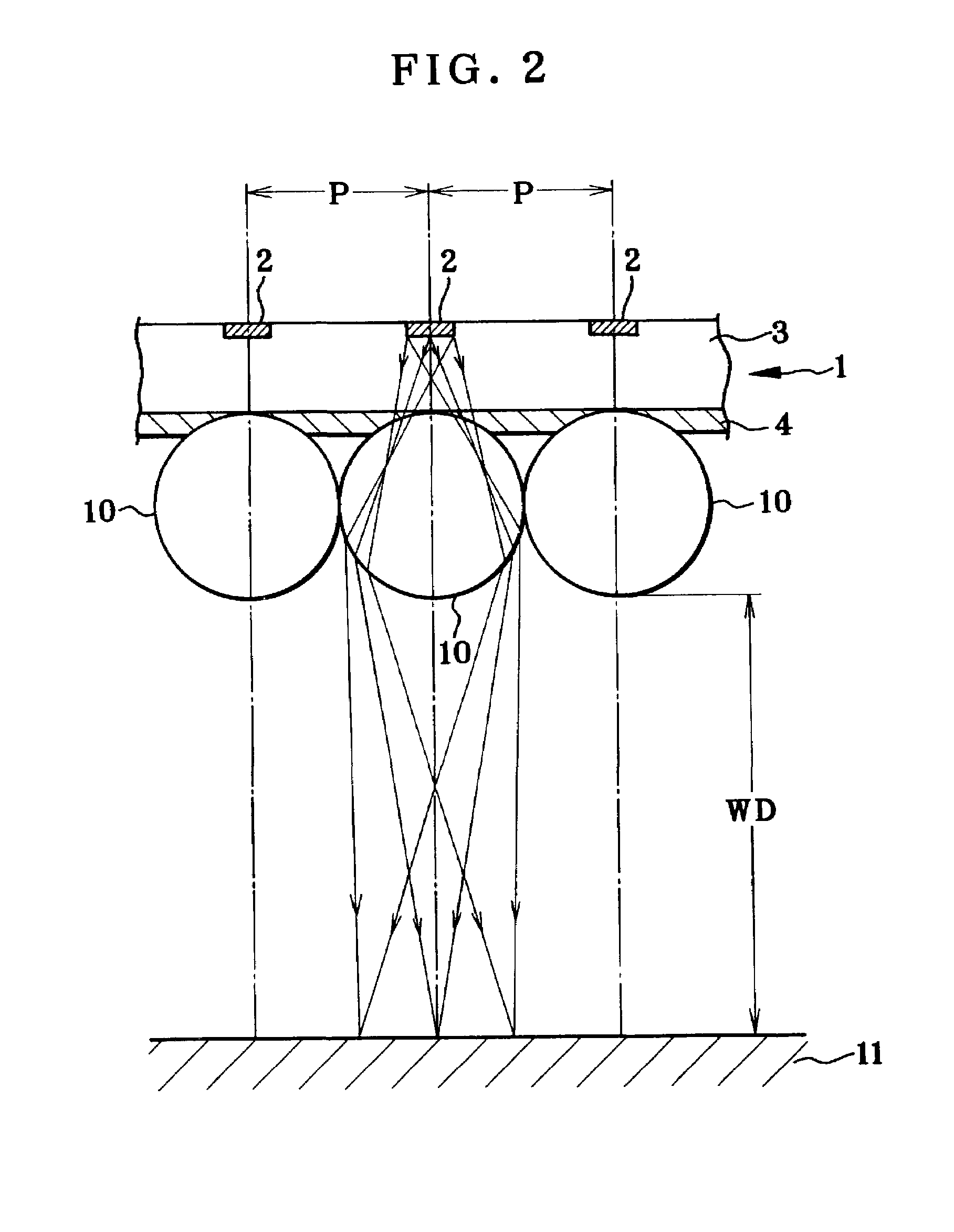
[0045]Further, in the optical writing head of the present invention achieving the second object, the barrier plate, having optical holes for preventing crosstalk of light i.e. a phenomenon that fluxes of light emitted from the light-emitting parts of adjacent organic EL elements are immixed at the condensing position of light from the light-emitting part of either organic EL element, is provided on the light-emitting side of the array of organic EL elements, thereby reducing the crosstalk between adjacent pixels and thereby obtaining enough resolution and contrast.
[0046]Still other objects and advantages of the invention will in part be obvious and will in part be apparent from the specification.
[0047]The invention accordingly comprises the features of construction, combinations of elements, and arrangement of parts which will be exemplified in the construction hereinafter set forth, and the scope of the invention will be indicated in the claims.

Problems solved by technology

However, the optical system for condensing the light-emitting parts to form an image on a photosensitive drum is not clear.
When an organic EL array is used as an exposure head of a printer such as an electrophotographic printer, in case of using a condensing rod lens array for condensing fluxes of light from light-emitting parts of the organic EL array or the LED array or from shutter parts of the liquid-crystal shutter array onto a photosensitive drum, the exposure head requires long optical path length and thus needs increase in size.
In addition, since the condensing rod lenses are not arranged in a one-on-one relation to the light-emitting parts or the shutter parts, periodical optical irregularity occurs.
Moreover, since the condensing rod lens requires advanced manufacturing technology, the increase in cost is inevitable.
In case that the organic EL array is integrated with microlenses, there are problems such as a restriction in usable microlens materials.
In case of using a microlense array, though the microsenses are arranged in a one-on-one relation to light-emitting parts, such crosstalk in which light from a light-emitting part is incident on a pixel position through a microlens, not a microlens corresponding to the light-emitting part, e.g. a microlens adjacent to the corresponding microlens easily occurs, thus leading to the reduction in resolution.

Method used


Image

  • Optical writing head such as organic EL array exposure head, method of manufacturing the same, and image forming apparatus using the same
  • Optical writing head such as organic EL array exposure head, method of manufacturing the same, and image forming apparatus using the same
  • Optical writing head such as organic EL array exposure head, method of manufacturing the same, and image forming apparatus using the same

Examples


Embodiment Construction

[0067]Hereinafter, an optical writing head achieving the first object of the present invention and a method of manufacturing the same will be described with regard to embodiments.

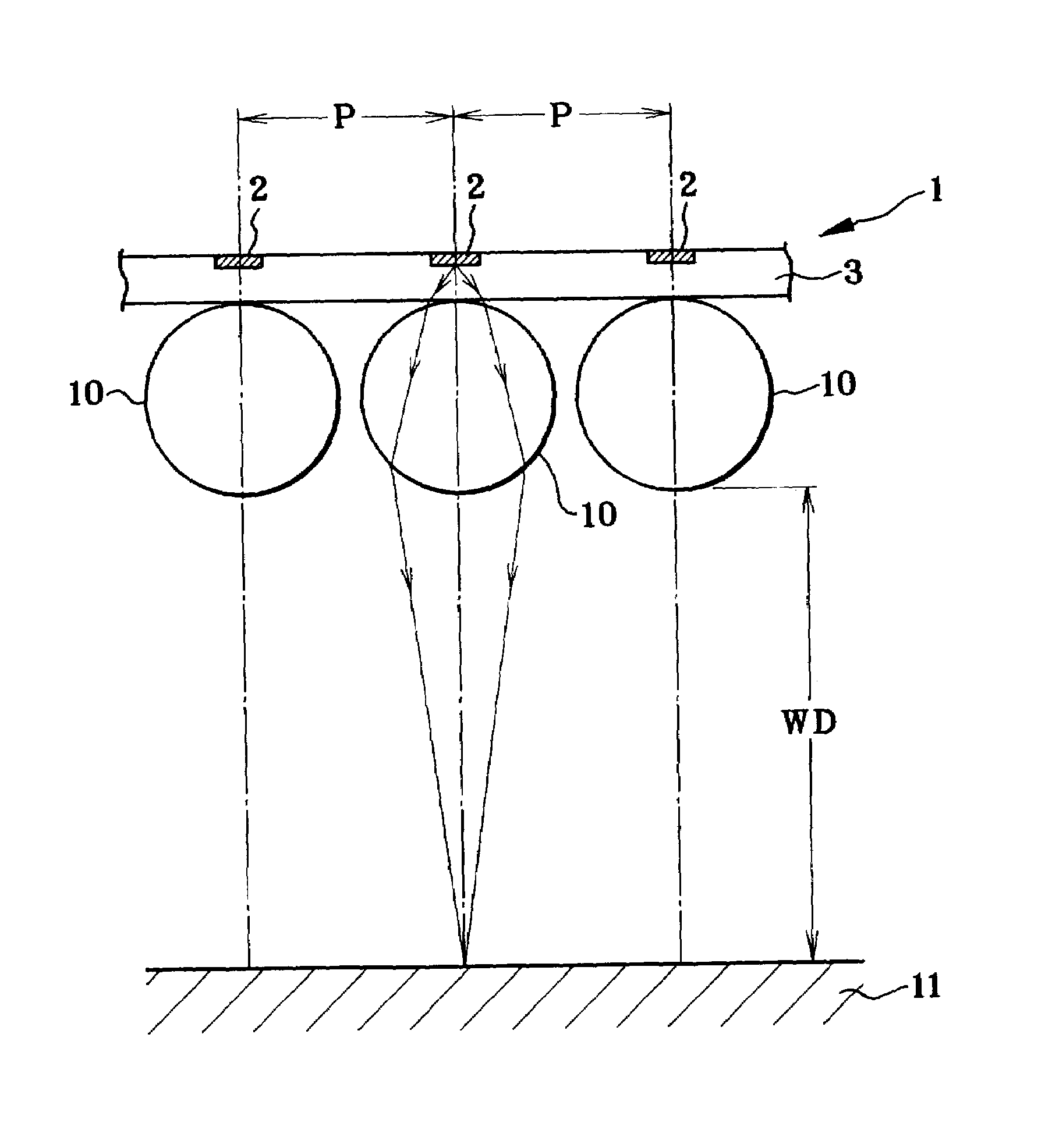
[0068]FIG. 1 is a sectional view schematically showing the basic structure of the optical writing head according to the present invention, in which light-emitting parts 2 such as organic EL and LED or shutter portions 2 such as a liquid crystal shutter are placed on the surface of or in a transparent layer 3 at constant interval, thereby forming a light-emitting element array 1 or an optical shutter element array 1. In case of the optical shutter element array 1, the shutter parts 2 per se do not emit light. However, light sources (backlight) are disposed behind the shatter parts 2 so that the shutter parts 2 function as secondary light source. Therefore, in the following description except for special explanation, the shutter parts 2 will be called the light-emitting parts 2 and, in addition, the light-emi...


PUM


Abstract

The present invention relates to a small optical writing head, such as an organic EL array exposure head, having long work distance with little crosstalk, a method of manufacturing the same, and an image forming apparatus using the same. The optical writing head is an optical writing head which projects fluxes of modulated light from light-emitting parts 2 of a light-emitting element array such as an organic EL array or fluxes of modulated light transmitted through shutter parts 2 of an optical shutter element array onto an image carrier 11 to form a predetermined pattern on the image carrier 11. The optical writing head comprises ball lenses 10 which are arranged such that the alignment of the ball lenses 10 corresponds to the alignment of the light-emitting parts 2 of the light-emitting element array or the shutter parts 2 of the optical shutter element array.

Description

BACKGROUND OF THE INVENTION[0001]The present invention relates to an optical writing head such as an organic electroluminescence (EL) array exposure head, a method of manufacturing the same, and an image forming apparatus using the same. More particularly, the present invention relates to an optical writing head comprising ball lenses arranged corresponding to elements of a light emitting element array such as organic EL array or a light shatter element array for condensing fluxes of light from the elements onto a photoreceptor, a method of manufacturing the same, and an image forming apparatus using the same.[0002]The present invention also relates to an organic EL array exposure head which is designed to prevent crosstalk between pixels, and an image forming apparatus using the same.[0003]Conventionally, various techniques of using an organic EL array as an exposure head for image forming apparatus have been proposed. Those concerned therewith are as follows.[0004]In Japanese Pate...

Claims


Application Information

Patent Timeline
IPC IPC(8): B41J27/00B41J2/45
CPCB41J2/451
Inventor SEKI, HIDEYAYONEKUBO, MASATOSHI
Owner SEIKO EPSON CORP
Learn More