Dynamic RAM storage techniques

a dynamic ram and storage technology, applied in the field of dram cells, can solve the problems of limiting the operating speed of the circuit, adversely affecting the operation of the pld, and requiring more circuitry, so as to reduce the collection volume of ionizing particles, prevent signal degradation, and reduce the effect of soft error

Inactive Publication Date: 2006-08-08
ALTERA CORP
View PDF21 Cites 31 Cited by
  • Summary
  • Abstract
  • Description
  • Claims
  • Application Information

AI Technical Summary

Benefits of technology

[0010]According to some embodiments, DRAM cells of the present invention can be used in memory arrays on a programmable integrated circuit (IC) to store configuration data. On a programmable IC, pass gates couple together different segments of programmable interconnect wires. Pass gates can be used to make multiplexers to bypass various logical functions. Data stored in the DRAM cells can be provided directly to the pass gates at the full value of the supply voltage to prevent signal degradation.
[0011]According to other embodiments, DRAM cells of the present invention are less sensitive to soft errors. A p-channel read access transistor is used to access data stored in the DRAM cell. The p-channel transistor eliminates all N-type junctions from the storage node reducing the collection volume of ionizing particles such as alpha particles and cosmic rays that may cause soft errors.

Problems solved by technology

This requires more circuitry and tends to limit the operating speed of the circuit.
The operation of a PLD is adversely effected when charge stored in memory is degraded during read cycles.

Method used


Image

  • Dynamic RAM storage techniques
  • Dynamic RAM storage techniques
  • Dynamic RAM storage techniques

Examples


Embodiment Construction

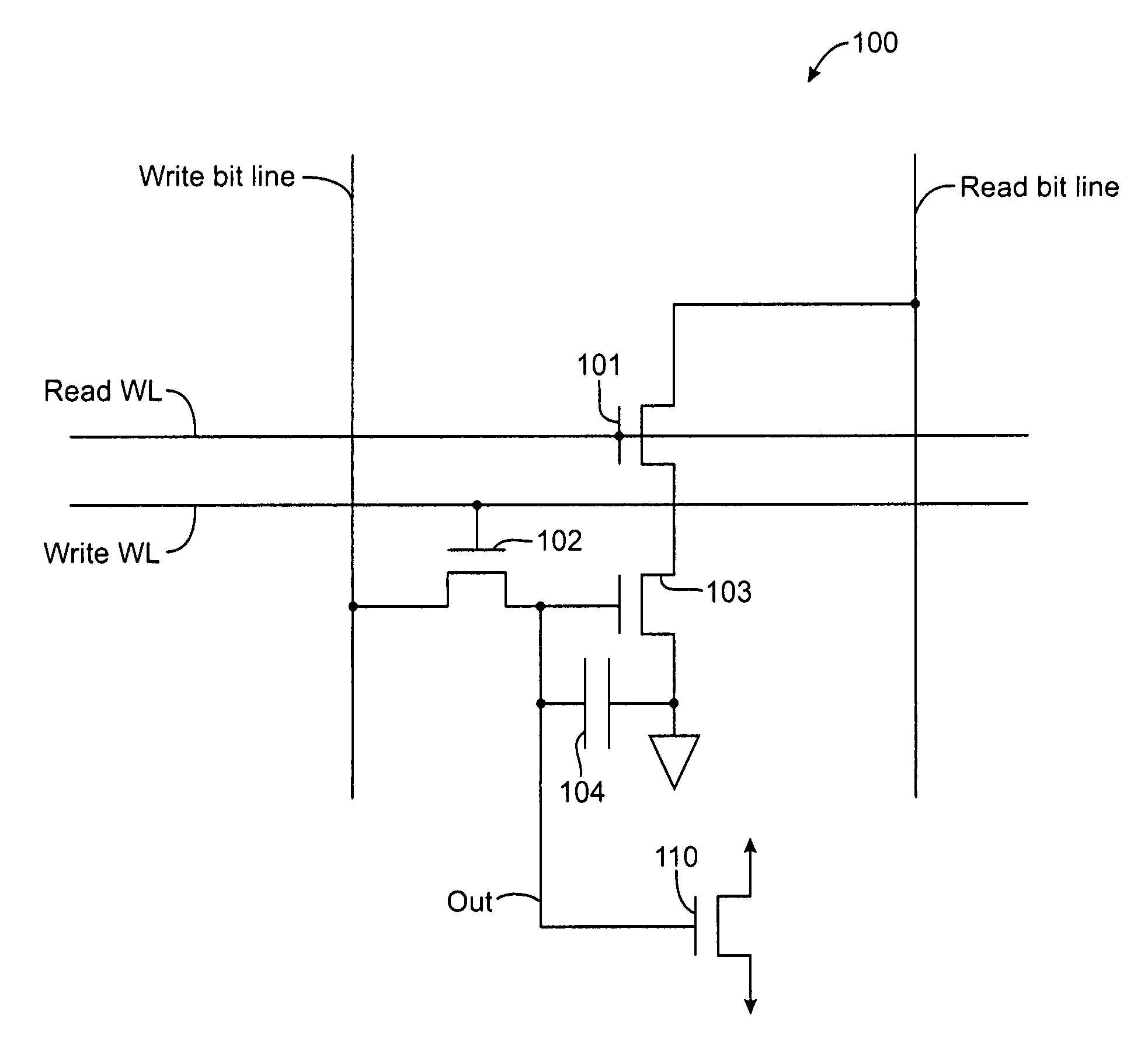
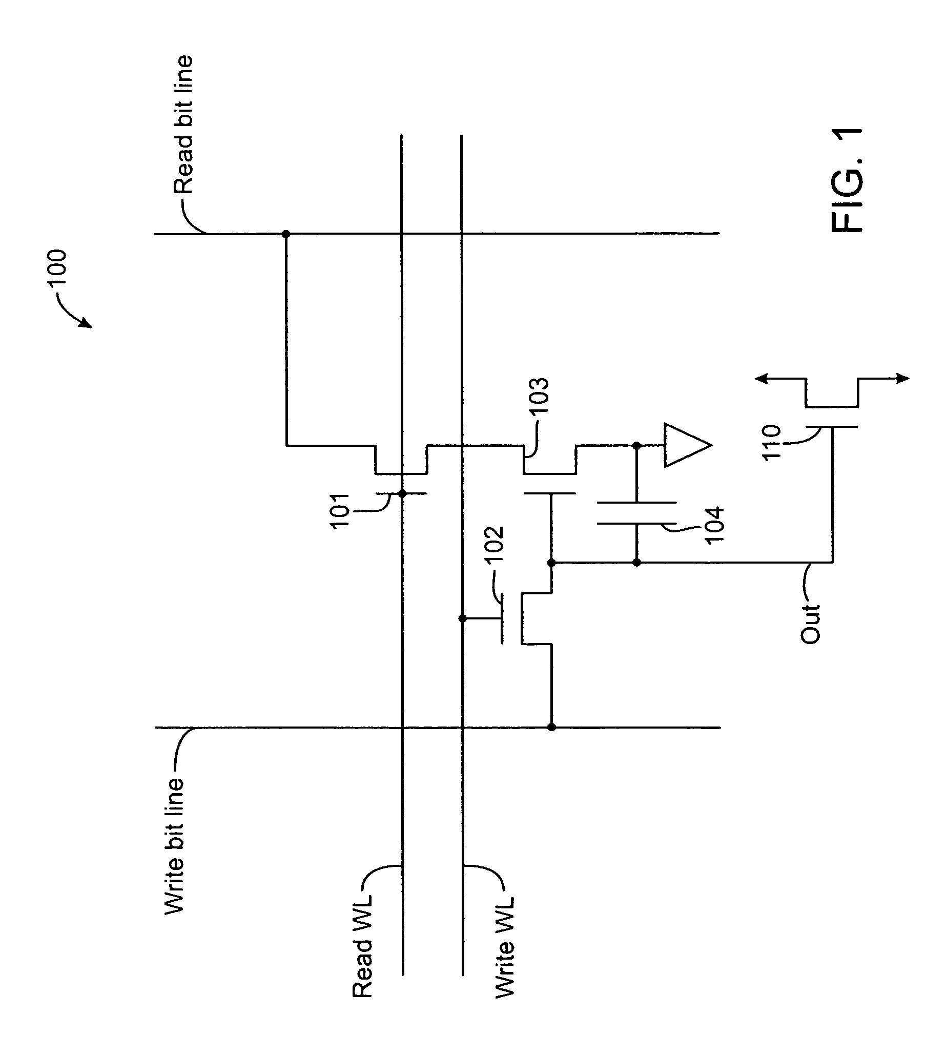
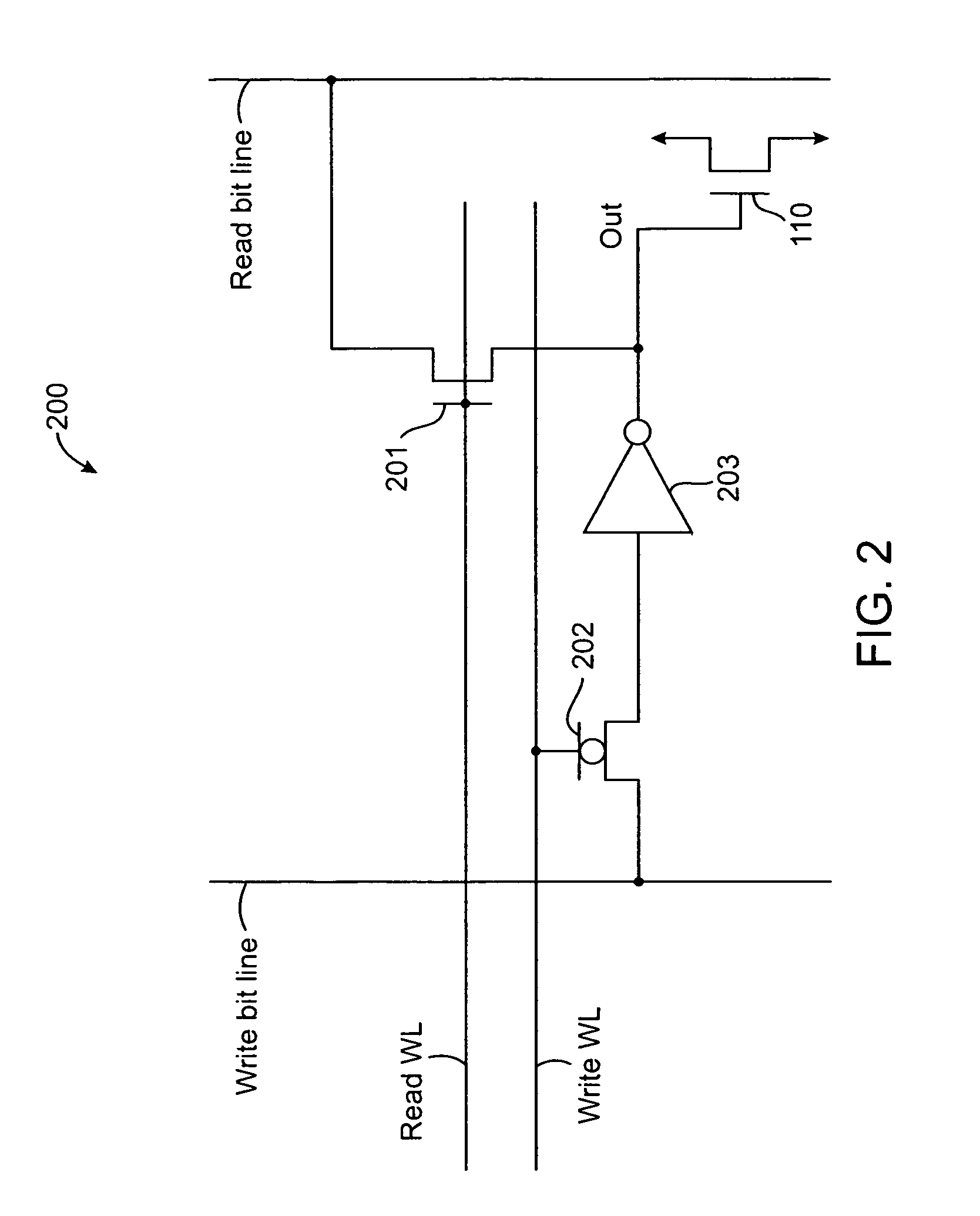
[0019]FIG. 1 illustrates a three transistor DRAM cell 100 according to a first embodiment of the present invention. DRAM cell 100 includes n-channel field effect transistors 101, 102, and 103. DRAM cell 100 also includes capacitor 104. The operation of DRAM cell 100 will now be described.

[0020]A data bit can be stored in DRAM cell 100 by raising the Write Word Line (WL) to the high supply voltage (VCC) to turn on transistor 102. When transistor 102 is on, the gate of transistor 103 is coupled to the Write Bit Line. Data can now be stored on capacitor 104 at the gate of transistor 103 by applying a selected voltage to the Write Bit Line. For example, the Write Bit Line can be driven to a logic high or a logic low to store a logic signal on capacitor 104.

[0021]Once a data bit has been stored in DRAM cell 100, the voltage on the Write Word Line is lowered to ground to turn off transistor 102. When transistor 102 is off, the stored voltage on capacitor 104 begins to decay. A periodic re...


PUM


Abstract

Dynamic RAM (DRAM) cells are provided. Data can be read from a DRAM cell without draining the stored charge stored in the cell. During a read cycle, current flows between a Read Bit line and a supply voltage, and charge is not drained directly from the DRAM storage node. Each DRAM cell has a small number of transistors. The DRAM cell can be used to store configuration data on a programmable integrated circuits (IC). Pass gates are used on programmable ICs to drive signals across the chip. Data stored in DRAM cells is provided directly to the pass gates at the full supply voltage to prevent signal degradation.

Description

BACKGROUND OF THE INVENTION[0001]The present invention relates to DRAM cells, and more particularly, to techniques for storing data in and accessing data from DRAM cells.[0002]Arrays of dynamic random access memory (DRAM) cells have been provided as an alternative to static random access memory (SRAM) storage technology. DRAMs require far less transistors than SRAM devices to store a given quantity of data bytes.[0003]A DRAM cell can be fabricated using standard CMOS technology or other well known types of processing technology. One type of DRAM cell includes a small storage capacitor coupled to a single access transistor. This DRAM cell is a much smaller cell than a typical SRAM cell.[0004]DRAM cells dynamically store data on storage capacitors. Because charge leaks from the capacitors, the cells must be refreshed periodically. A typical DRAM refresh cycle includes the steps of addressing the cells, sensing their contents (i.e. logic high or logic low), and writing the information ...

Claims


Application Information

Patent Timeline
Patent Type & Authority Patents(United States)
IPC IPC(8): G11C11/24G11C11/405G11C11/406
CPCG11C5/005G11C7/02G11C11/405G11C11/406G11C11/4094G11C11/4097G11C11/4085G11C2211/4065G11C2207/104
Inventor TURNER, JOHN
Owner ALTERA CORP
Why Eureka
Try Eureka