Electronic device including dielectric layer, and a process for forming the electronic device

a technology of electronic devices and dielectric layers, applied in the direction of semiconductor/solid-state device details, chemical vapor deposition coatings, coatings, etc., can solve the problems of undesired interfaces, degraded reliability, and undesired addition of divalent or trivalent impurities to hfo/sub>2 or zro/sub>2

Active Publication Date: 2006-08-15
NXP USA INC
View PDF13 Cites 59 Cited by
  • Summary
  • Abstract
  • Description
  • Claims
  • Application Information

AI Technical Summary

Problems solved by technology

A MISFET having an HfO2 gate dielectric layer suffers from a relatively lower mobility of carriers within the MISFET's channel region and degraded reliability.
The interface(s) are undesired because they are more likely to have defects, trapped charge, or a combination thereof at the interface(s) as opposed to a gate dielectric layer that is not a laminate.
Therefore, adding a divalent or trivalent impurity to HfO2 or ZrO2 is undesired.
Separating the two from each other can be difficult.

Method used


Image

  • Electronic device including dielectric layer, and a process for forming the electronic device
  • Electronic device including dielectric layer, and a process for forming the electronic device
  • Electronic device including dielectric layer, and a process for forming the electronic device

Examples


Embodiment Construction

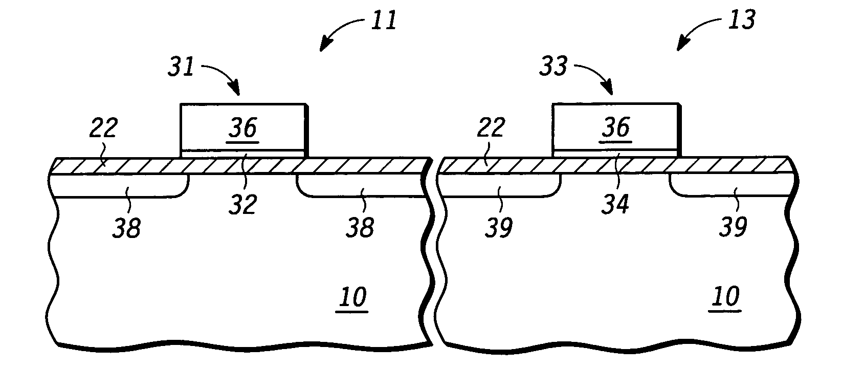
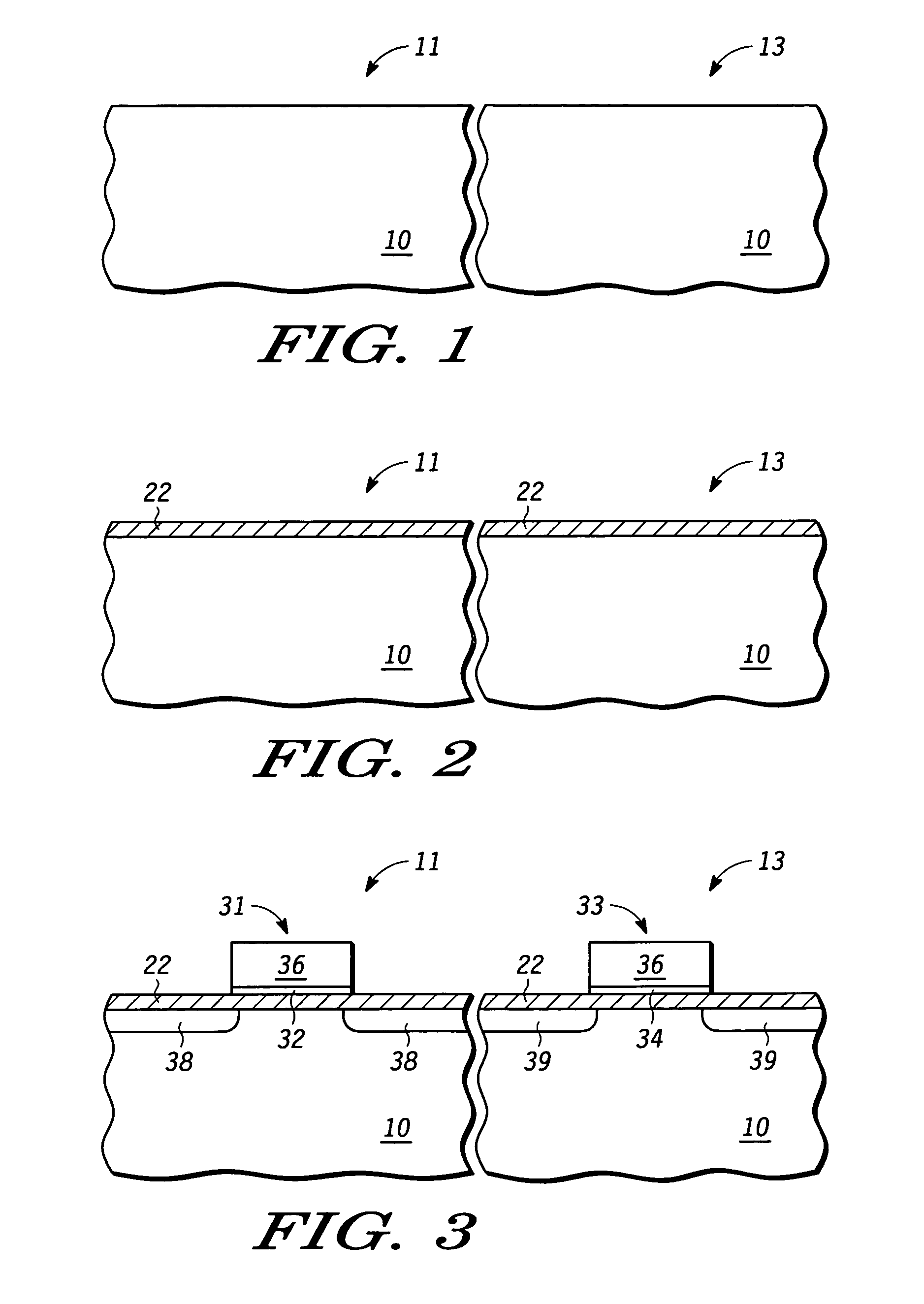
[0015]A mixture of materials can be used within a layer of an electronic device to improve electrical and physical properties of the layer. In one set of embodiments, the layer can be a dielectric layer, such as a gate dielectric layer or a capacitor dielectric layer. The dielectric layer can include oxygen, and two or more dissimilar metallic elements. In one specific embodiment, two dissimilar elements may have the same single oxidation state and be miscible within each other. In one embodiment, the dielectric layer can include an alloy of (HfO2)(1-x)(ZrO2)x, wherein x has a value between 0 and 1. Each of Hf and Zr has a single oxidation state of +4. Other combinations are possible. Improved electrical and physical properties can include better control over grain size, distribution of grain sizes, thickness of the layer across a substrate, improved carrier mobility, threshold voltage stability, or any combination thereof.

[0016]In one embodiment, a dielectric layer includes oxygen,...


PUM

PropertyMeasurementUnit
atomic numbersaaaaaaaaaa
thicknessaaaaaaaaaa

Abstract

A mixture of materials can be used within a layer of an electronic device to improve electrical and physical properties of the layer. In one set of embodiments, the layer can be a dielectric layer, such as a gate dielectric layer or a capacitor dielectric layer. The dielectric layer can include O, and two or more dissimilar metallic elements. In one specific embodiment, two dissimilar elements may have the same single oxidation state and be miscible within each other. In one embodiment, the dielectric layer can include an alloy of (HfO2)(1-x)(ZrO2)x, wherein x is between 0 and 1. Each of Hf and Zr has a single oxidation state of +4. Other combinations are possible. Improved electrical and physical properties can include better control over grain size, distribution of grain sizes, thickness of the layer across a substrate, improved carrier mobility, threshold voltage stability, or any combination thereof.

Description

BACKGROUND[0001]1. Field of the Disclosure[0002]The present disclosure relates to dielectric layers, electronic devices, and processes, and more particularly to a dielectric layer including a metallic oxide, an electronic device comprising the dielectric layer, and an electronic device including a layer that includes grains.[0003]2. Description of the Related Art[0004]State-of-the-art metal-insulator-semiconductor field-effect transistors (MISFETs) require gate dielectric layers having a relatively high dielectric constant (“high-k”). For the purposes of this specification, a high-k material has a dielectric constant higher than silicon nitride, which is approximately seven. One such material is HfO2. A MISFET having an HfO2 gate dielectric layer suffers from a relatively lower mobility of carriers within the MISFET's channel region and degraded reliability.[0005]One attempt to address the shortcomings of an HfO2 gate dielectric layer is to use a laminated gate dielectric layer that...

Claims


Application Information

Patent Timeline
Patent Type & Authority Patents(United States)
IPC IPC(8): H01L29/76H01L21/8242
CPCC23C16/45529C23C16/45531H01L21/28185H01L21/28194H01L21/28229H01L29/517H01L21/31641H01L21/31645H01L21/823842H01L21/3141H01L29/4966H01L21/02194H01L21/02189H01L21/02181
Inventor HEGDE, RAMA I.DEMKOV, ALEXANDER A.TOBIN, PHILIP J.TRIYOSO, DINA H.
Owner NXP USA INC
Why Eureka
Try Eureka