Spectrophotometer

a spectrophotometer and integrated technology, applied in the field of spectrophotometers, to achieve the effect of stable measurement, reliable and inexpensive, and small siz

Inactive Publication Date: 2006-08-15
OLYMPUS CORP
View PDF3 Cites 45 Cited by
  • Summary
  • Abstract
  • Description
  • Claims
  • Application Information

AI Technical Summary

Benefits of technology

[0008]It is an object of the present invention to provide a spectrophotometer which provides high-level performance capable of stable measurement and at the same time is reliable and inexpensive, while maintaining its small size and accuracy of positioning between optical component parts. It is another object of the invention to provide a spectrophotometer having an optimum optical element substrate and optical element. It is yet another object of the invention to provide a spectrophotometer having an optimum photoelectric conversion device substrate and photoelectric conversion device. It is a further object of the invention to provide a spectrophotometer having an optimum optical waveguide board. It is another object of the invention to provide a spectrophotometer having an optimum connection means between the optical waveguide board and the photoelectric conversion device substrate. It is still another object of the invention to provide a spectrophotometer which is capable of efficiently using incident light.

Problems solved by technology

Those spectrophotometers combining optical component parts have the problems of how to rectify shift in the positioning alignment between the optical component parts to improve wavelength accuracy and how to reduce size thereof.

Method used


Image

  • Spectrophotometer
  • Spectrophotometer
  • Spectrophotometer

Examples


first embodiment

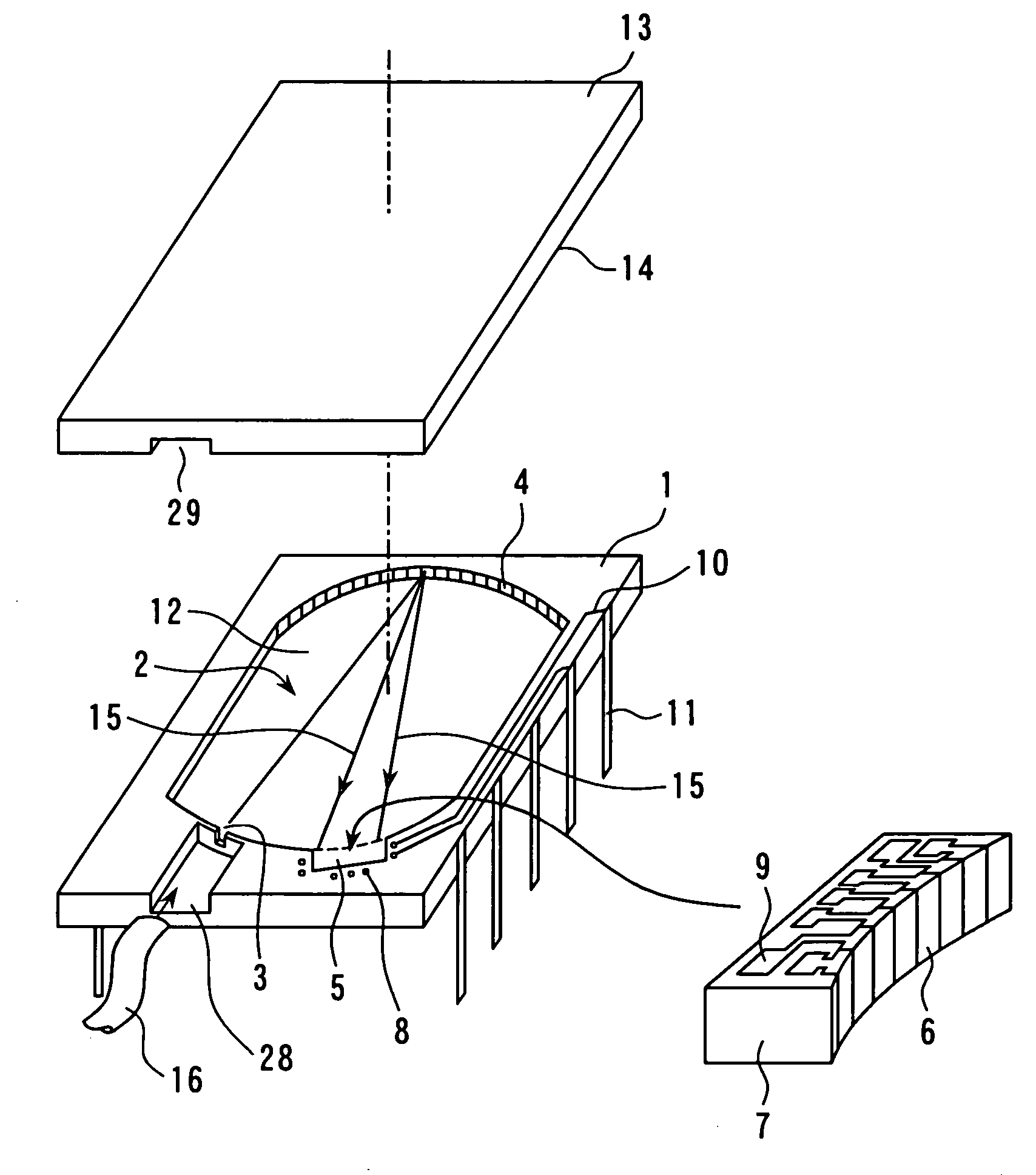
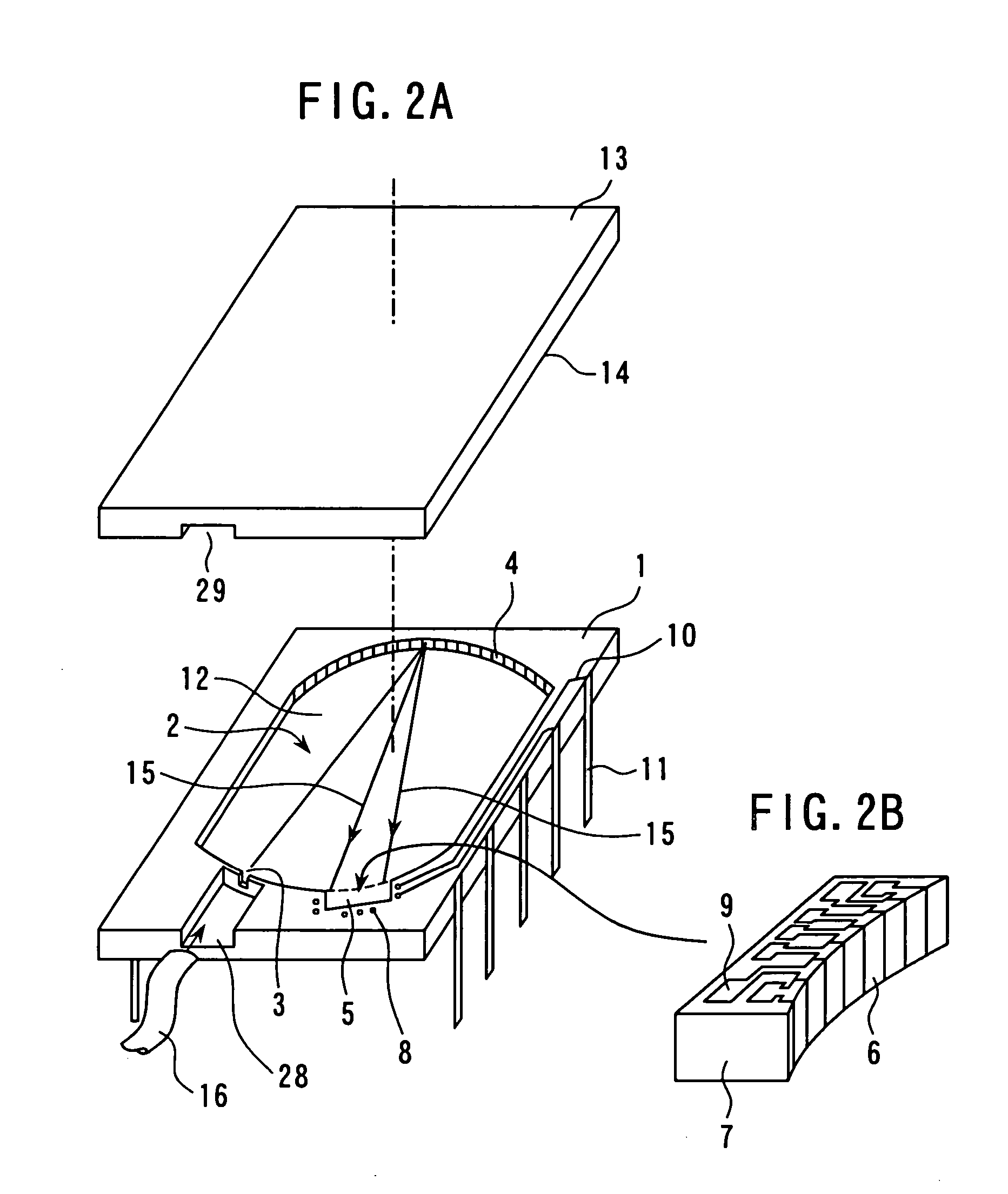
[0039]Some embodiments of the spectrophotometer according to the invention will be described in the following. A first embodiment will now be described. FIG. 2A is a disassembled perspective view showing the first embodiment of the spectrophotometer according to the invention. Referring to FIG. 2A, what is denoted by numeral 1 is an optical waveguide board having thereon an optical waveguide 2 of which a portion is processed into a concave. A metal, ceramic, or plastic, for example, may be used as the material of the optical waveguide board 1. Though its material is not limited, a board made of plastic is used here. Denoted by numeral 3 is a light entrance slit formed on an end face of the optical waveguide 2, i.e., a stepped end face portion of the optical waveguide board 1; 4 is a diffraction grating serving as optical element formed on an end face portion of the optical waveguide 2 facing the light entrance slit 3; 5 is a mounting portion for photoelectric conversion device forme...

second embodiment

[0049]A second embodiment of the spectrophotometer according to the invention will now be described. In the present embodiment, the electrical connection means between the photoelectric conversion device substrate and the optical waveguide board is formed in another manner different from the above described first embodiment. FIG. 9 shows main portions of the second embodiment of the spectrophotometer according to the invention. In particular, FIG. 9 is a disassembled perspective view as seen from the incidence side of the manner of mounting on the optical waveguide board 1 the photoelectric conversion device substrate 7 on which the photodiode array 6 is disposed. Those components corresponding to those in the first embodiment shown in FIG. 3 are denoted by identical reference numerals.

[0050]As shown in FIG. 9, the electrode pad 8 of the optical waveguide board side is provided on the bottom portion of the photoelectric conversion device mounting portion 5 of the optical waveguide b...

third embodiment

[0053]A third embodiment according to the invention will now be described. In the present embodiment, the construction of the light receiving surface of the photodiode array is different from the first and second embodiments. As a result, the manner of electrical connection between the photoelectric conversion device substrate and the optical waveguide board is different. The construction of other portions is similar to that of the first embodiment. FIGS. 10A to 10D are a disassembled perspective view showing the third embodiment of the spectrophotometer according to the invention. Like components as in the first embodiment shown in FIGS. 2A and 2B are denoted by like reference numerals.

[0054]As shown in FIG. 10A, a photoelectric conversion device substrate 7 is prepared such that a plate-like photoelectric conversion device substrate portion having the photodiode array 6 and its receiving surface formed on a surface thereof is formed into a thin film for example by polishing or etc...


PUM


Abstract

Disclosed herein is a spectrophotometer at least including: an optical waveguide; a light entrance slit provided at an end face on the inner side of the optical waveguide, for bringing an incident light into the optical waveguide; an optical element provided at an end face on the inner side of the optical waveguide or at an interior of the optical waveguide, for separating the incident light brought in the optical waveguide into a spectrum; and a photoelectric conversion device provided at an end face on the inner side of the optical waveguide, for detecting the incident light separated into the spectrum at the optical element; wherein the optical waveguide, the light entrance slit, and the optical element being integrally formed on an optical waveguide board, and a photoelectric conversion device substrate having the photoelectric conversion device formed thereon being mounted on the optical waveguide board.

Description

[0001]This application claims benefit of Japanese Patent Application No. 2003-98804 filed in Japan on Apr. 2, 2003, the contents of which are incorporated by this reference.BACKGROUND OF THE INVENTION[0002]The present invention relates to spectrophotometers, and more particularly relates to a small-size integrated spectrophotometer.[0003]Spectrophotometers are used in many analyzing apparatus such as an analyzing apparatus for biochemistry. Those spectrophotometers combining optical component parts have the problems of how to rectify shift in the positioning alignment between the optical component parts to improve wavelength accuracy and how to reduce size thereof. As a solution to these problems, a technique concerning one-chip spectrophotometer has been proposed in Japanese patent application laid-open No. 2001-340309 by the present applicant.[0004]Shown in FIG. 1 is a disassembled perspective view of the small-size spectrophotometer as proposed in the above Japanese patent applic...

Claims


Application Information

Patent Timeline
Patent Type & Authority Patents(United States)
IPC IPC(8): G01J3/28G01J3/20G01J3/02G02B5/18H01L31/02
CPCG01J3/02G01J3/2803G01J3/0259G01J3/0256
Inventor SHIMIZU, ETSUROKOMINE, HITOSHI
Owner OLYMPUS CORP
Why Eureka
Try Eureka