Method of erasing NAND flash memory device

a technology of nand flash memory and nand flash, which is applied in the direction of solid-state devices, transistors, instruments, etc., can solve the problems of inability to erase memory cells to be programmed, increased leakage current generation, and inability to erase memory cells

Inactive Publication Date: 2006-08-22
STMICROELECTRONICS SRL +1
View PDF4 Cites 29 Cited by
  • Summary
  • Abstract
  • Description
  • Claims
  • Application Information

AI Technical Summary

Benefits of technology

[0009]The present invention is directed to solve the aforementioned problem, providing a method of erasing a NAND flash memory device capable of restraining an erasing disturbance fail by preventing a leakage current from applying a negative voltage to a well of a high voltage transistor forming an X-decoder.

Problems solved by technology

However, when a high voltage transistor employed in an X-decoder is conditioned in an abnormal state, a leakage current is generated and increases up to several tens through hundreds pA / μm.
Therefore, when the leakage current makes a voltage boosted for a control gate of a memory cell down more than 7V from its original voltage level, it causes a disturbance effect in a deselected cell block and then results in a serious problem that memory cells to be programmed are undesirably forced to be erased.

Method used


Image

  • Method of erasing NAND flash memory device
  • Method of erasing NAND flash memory device
  • Method of erasing NAND flash memory device

Examples


Embodiment Construction

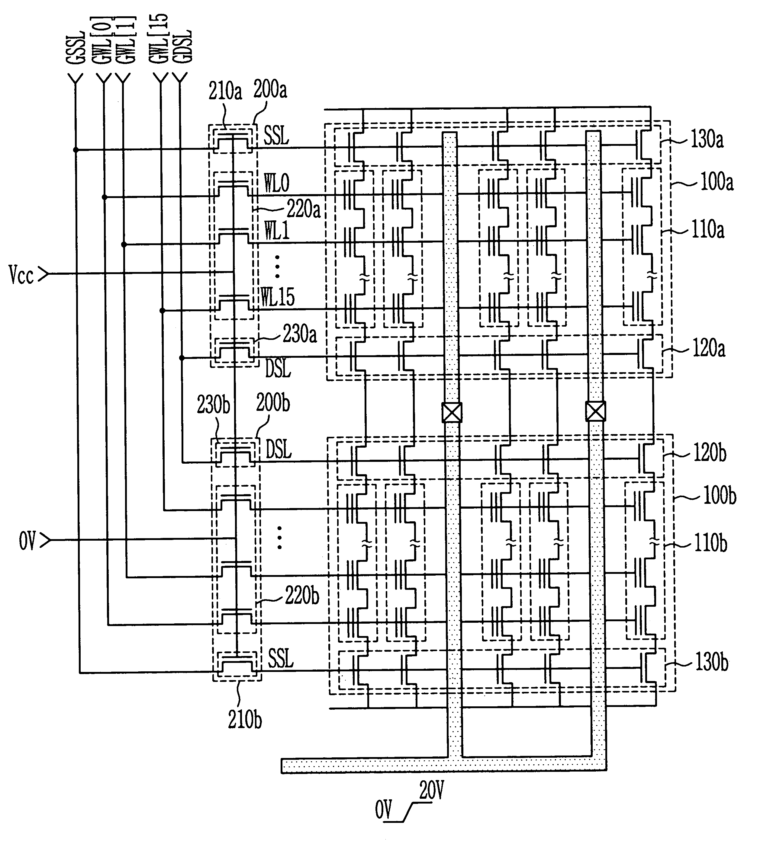
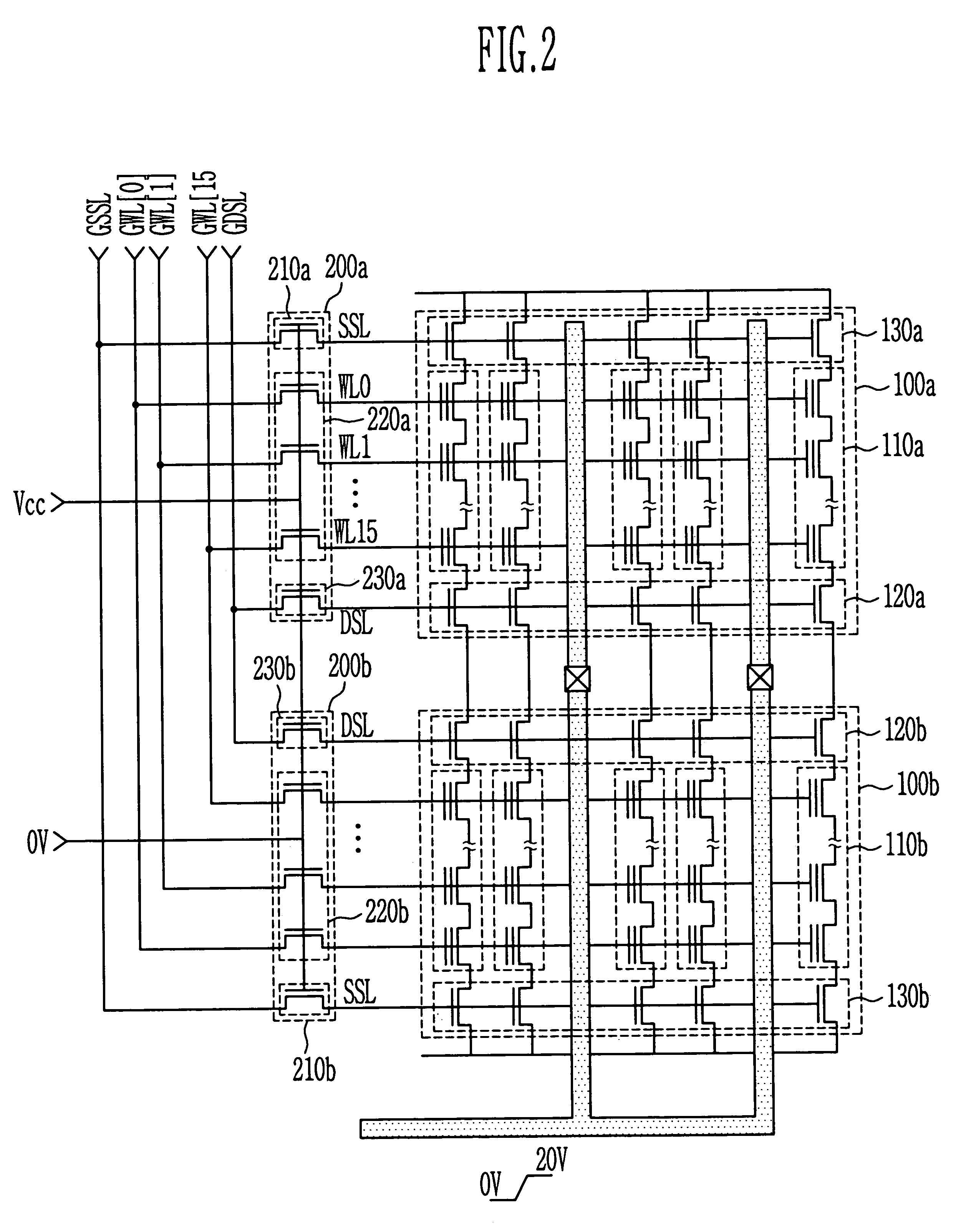
[0019]Preferred embodiments of the present invention will be described below in more detail with reference to the accompanying drawings. The present invention may, however, be embodied in different forms and should not be constructed as limited to the embodiments set forth herein. Rather, these embodiments are provided so that this disclosure will be thorough and complete, and will fully convey the scope of the invention to those skilled in the art. Like numerals refer to like elements throughout the specification.

[0020]Hereinafter, it will be described about an exemplary embodiment of the present invention in conjunction with the accompanying drawings.

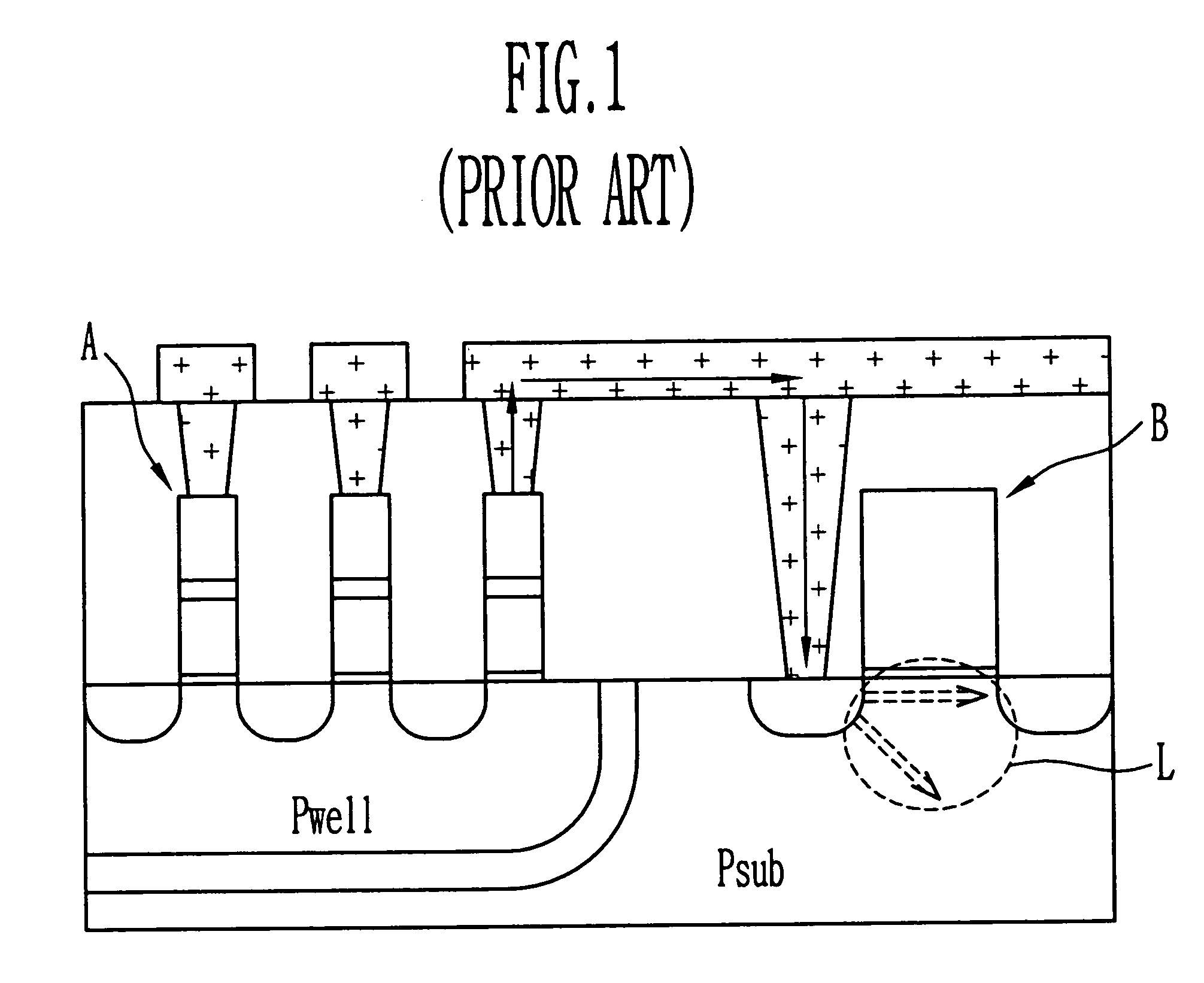
[0021]In order to regulate a leakage current generated from a high voltage transistor used in a conventional X-decoder less than 1 pA / μm, it may be required to set a threshold voltage of the high voltage transistor over 0.75 V or to use a negative voltage therein.

[0022]First, considering the case of elevating the threshold voltage of ...


PUM


Abstract

Provided is concerned with a method of erasing a NAND flash memory device, capable of restraining an erasing disturbance fail arising from a deselected cell block and improving a product yield of the device by applying a negative voltage to a well of a high voltage transistor forming an X-decoder during an erasing operation in the NAND flash memory device.

Description

BACKGROUND[0001]1. Field of the Invention[0002]The present invention is related to a method of erasing a NAND flash memory device and particularly, to a method of erasing which is able to improve a protecting function for erasing disturbance fails.[0003]2. Discussion of Related Art[0004]Data stored in a NAND flash memory device is erased in the unit of block. During this, there is no disturbance because a non-erased block is boosted such that a wordline of memory cells is supplied with 20V that is offset with a well bias 20V.[0005]However, when a high voltage transistor employed in an X-decoder is conditioned in an abnormal state, a leakage current is generated and increases up to several tens through hundreds pA / μm. As a result, the bias voltage of 20V boosted at a gate of a non-erased memory cell decreases under 13V, so that information stored in the memory cell is lost due to disturbance by an erasing bias voltage of 20V set in a sell of a memory cell array.[0006]FIG. 1 is a sche...

Claims


Application Information

Patent Timeline
Patent Type & Authority Patents(United States)
IPC IPC(8): G11C11/34G11C16/02G11C16/06G11C16/04G11C16/14G11C16/16H01L21/8247H01L27/115H01L29/788H01L29/792
CPCG11C16/16E03C1/052
Inventor LEE, KEUN WOO
Owner STMICROELECTRONICS SRL
Why Eureka
Try Eureka