Masked sidewall implant for image sensor

a sidewall implant and image sensor technology, applied in semiconductor devices, diodes, electrical devices, etc., can solve problems such as current leakage and performance deficiencies of collection diodes

Active Publication Date: 2006-08-29
SMARTSENS TECH (HK) CO LTD
View PDF17 Cites 6 Cited by
  • Summary
  • Abstract
  • Description
  • Claims
  • Application Information

AI Technical Summary

Benefits of technology

[0009]It is thus an object of the present invention to provide a novel structure and method of forming an imaging device cell structure that ensures a proper electrical connection between the surface pinning layer of the collection well device and the underlying substrate.
[0010]It is a further object of the present invention to provide an imaging sensor device APS cell structure that includes an adjacent isolation (STI) structure including a sidewall edge and that is provided with a novel sidewall implant region for ensuring improved alignment of conductive material and proper electrical contact between the surface pinning layer above the collection well device and the underlying substrate.
[0011]It is a further object of the present invention to provide an implant doping technique in a method for manufacturing an image sensor APS cell including an adjacent isolation STI structure that replaces the underlying well implant with an implant into the sidewall of the STI region to ensure improved alignment of conductive material and proper electrical contact between the surface pinning layer above the collection well device and the underlying substrate.

Problems solved by technology

This tolerance is depicted by the double-sided arrow shown in FIG. 1 and results in potentially misalignment of the connection leading to collection diode device performance deficiencies such as current leakage.

Method used


Image

  • Masked sidewall implant for image sensor
  • Masked sidewall implant for image sensor
  • Masked sidewall implant for image sensor

Examples


Embodiment Construction

[0029]According to one aspect of the invention, there is provided an improved implant doping technique in a method for manufacturing an imaging device APS cell that ensures proper electrical connection between the surface pinning layer of the collection well device and the underlying substrate.

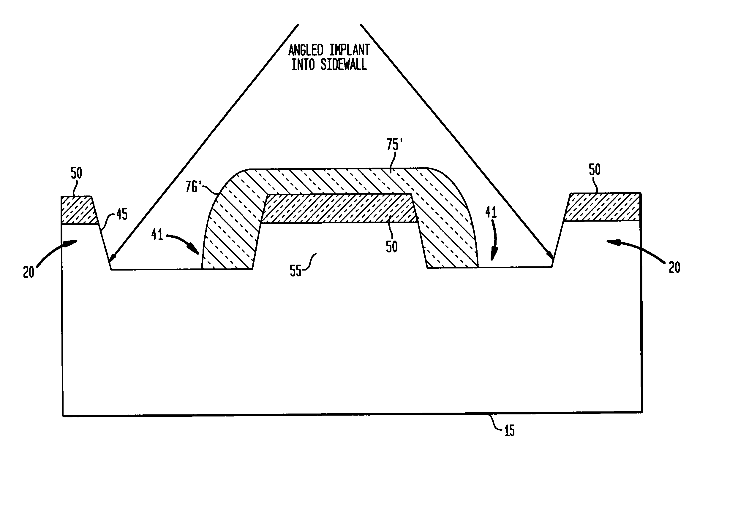
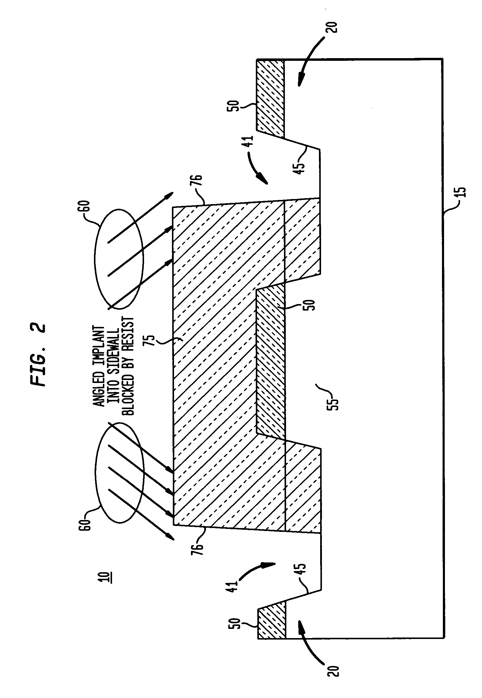
[0030]As shown in FIG. 2, there is provided a novel method in an APS cell manufacturing process that includes the application of block masks to perform an angled implant into a sidewall edge 45 of an adjacent formed STI trench region 41 associated with the APS cell 10 having a pinned photodiode 20. As will be explained in greater detail, a sidewall implant of the STI ensures that the eventual formed surface pinning layer of the pinned photodiode 20 is in electrical contact with the underlying substrate 15. In the process of forming the APS cell structure 10 of FIG. 2, STI trench regions 41 are first formed in a bulk semiconductor substrate including, for example, Si, SiGe, SiC, SiGeC, GaAs, In...


PUM


Abstract

A novel image sensor structure formed on a substrate of a first conductivity type includes a photosensitive device of a second conductivity type and a surface pinning layer of the first conductivity type. A trench isolation region is formed adjacent to the photosensitive device pinning layer. The structure includes a dopant region comprising material of the first conductivity type formed along a sidewall of the isolation region that is adapted to electrically couple the pinning layer to the substrate. The corresponding method facilitates an angled ion implantation of dopant material in the isolation region sidewall by first fabricating the photoresist layer and reducing its size by removing a corner, or a corner portion thereof, which may block the angled implant material. To facilitate the angled implant to the sidewall edge past resist block masks, two methods are proposed: 1) a spacer type etch of the imaged photoresist; or, 2) a corner sputter process of the imaged photoresist.

Description

CROSS REFERENCE TO RELATED APPLICATIONS[0001]The present invention is related to commonly-owned, co-pending U.S. patent application Ser. No. 10 / 904,896 (BUR920040218US1) entitled A PREDOPED TRANSFER GATE FOR AN IMAGE SENSOR and (BUR920040222US1) entitled A RECESSED GATE FOR AN IMAGE SENSOR, the whole contents and disclosure of each of which is incorporated by reference as if fully set forth herein.FIELD OF THE INVENTION[0002]The present invention relates generally to the fabrication of semiconductor pixel imager arrays, and more particularly, to a novel Active Pixel Sensor (APS) cell structure including a masked sidewall implant and process therefor.BACKGROUND OF THE INVENTION[0003]CMOS image sensors are beginning to replace conventional CCD sensors for applications requiring image pick-up such as digital cameras, cellular phones, PDA (personal digital assistant), personal computers, and the like. Advantageously, CMOS image sensors are fabricated by applying present CMOS fabricating...

Claims


Application Information

Patent Timeline
Patent Type & Authority Patents(United States)
IPC IPC(8): H01L21/00
CPCH01L27/1463H01L27/14689H01L27/14687H01L27/14643
Inventor ADKISSON, JAMES W.JAFFE, MARK D.JOHNSON, ARTHUR P.LEIDY, ROBERT K.MALING, JEFFREY C.
Owner SMARTSENS TECH (HK) CO LTD
Why Eureka
Try Eureka