Light emitting device, method of preparing the same and device for fabricating the same

a technology of light emitting devices and semiconductors, applied in the field of semiconductor devices, can solve problems such as the increase of pixels, and achieve the effects of reducing the size of the device, enhancing the aperture efficiency, and enhancing the reliability

Inactive Publication Date: 2006-08-29
SEMICON ENERGY LAB CO LTD
View PDF60 Cites 39 Cited by
  • Summary
  • Abstract
  • Description
  • Claims
  • Application Information

AI Technical Summary

Benefits of technology

[0015]Moreover, as a flat panel display of full colors using red, green and blue, the requirements for a high definition, a high aperture efficiency and a high reliability has been heightened. Such requirements have been big problems in seeking for the high definition (increase of the number of pixels) of a light emitting device and miniaturization of the respective display pixel pitch accompanied with downsizing of the device. Moreover, at the same time, the requirements for the enhancement of the productivity and the lowering of the cost have b

Problems solved by technology

Such requirements have been big problems in seeking for the high definition (increase of the number of pixels) of a lig

Method used


Image

  • Light emitting device, method of preparing the same and device for fabricating the same
  • Light emitting device, method of preparing the same and device for fabricating the same
  • Light emitting device, method of preparing the same and device for fabricating the same

Examples


embodiment 1

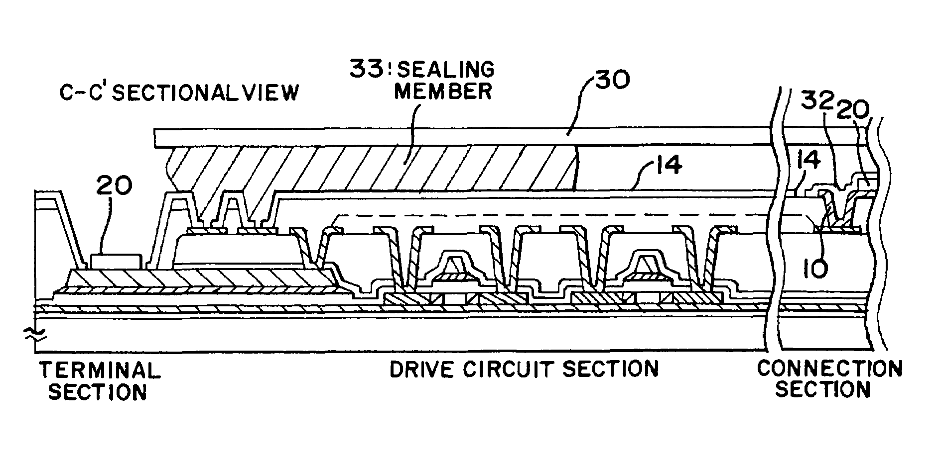
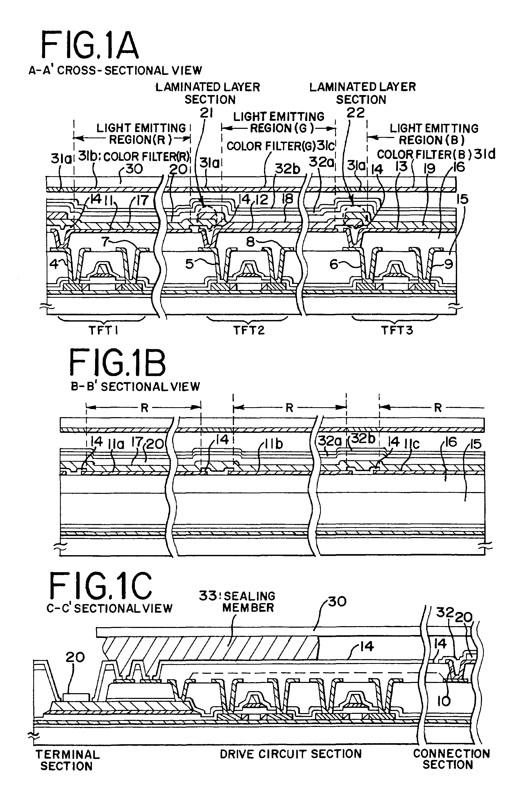
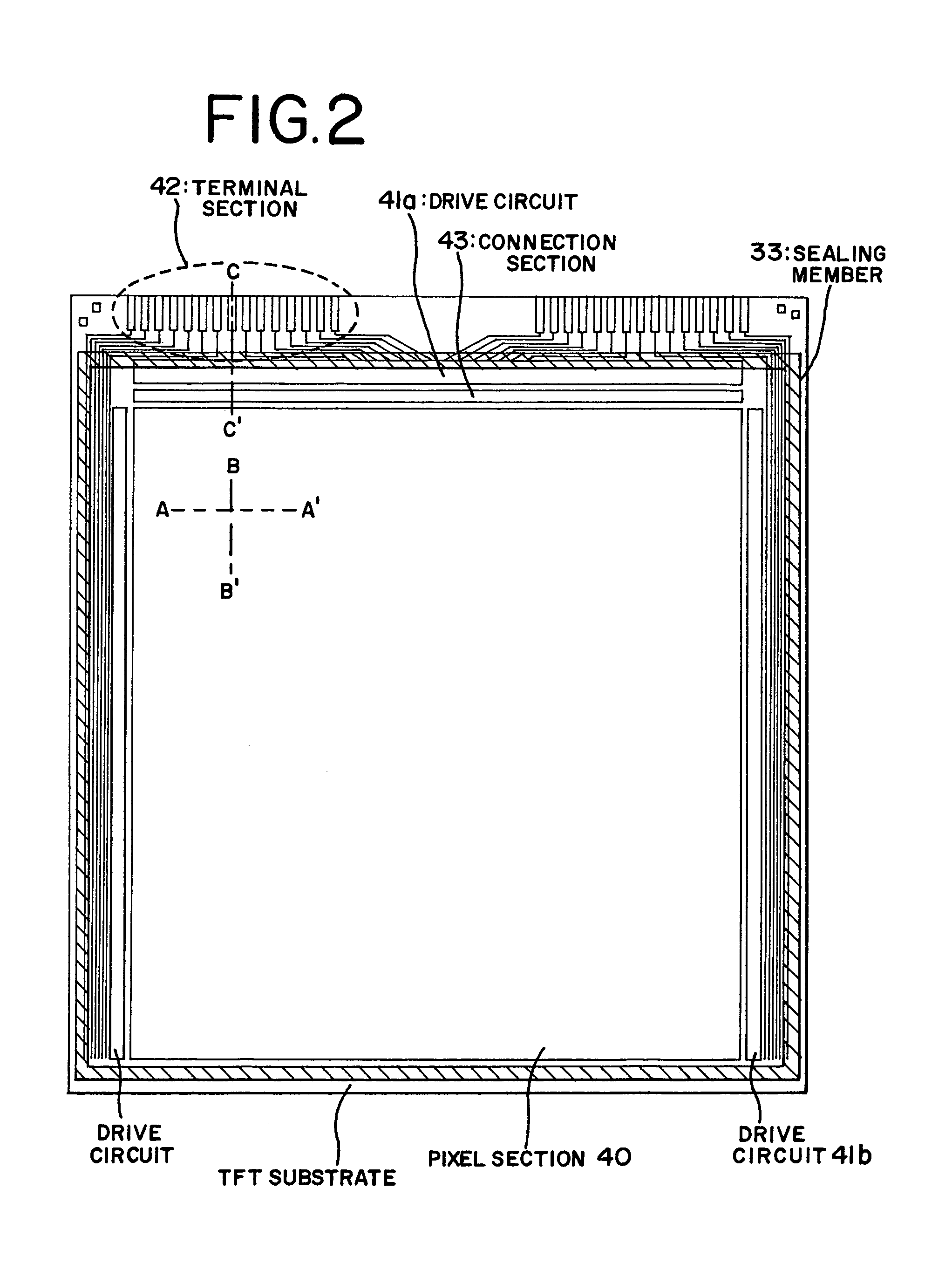
[0104]FIG. 2 is a top view of an EL module. On a substrate (referred to as TFT substrate) on which many TFTs are provided, a pixel section 40 where the display is performed, drive circuits 41a, 41b for driving the respective pixels of the pixel section, a connection section 43 connecting an electrode provided on the EL layer and the drawing wiring, and a terminal section 42 for pasting FPC for connecting with the exterior circuit are provided. Moreover, the EL element is sealed with a substrate for sealing the EL element and a sealing member 33. Moreover, FIG. 1A is a sectional view taken on chain line A–A′ of FIG. 2.

[0105]The pixels are disposed in order in the direction of the chain line A–A′, now, an example in which R, G and B in turn are disposed in the X direction is exemplified. In the present invention, as shown in FIG. 1A, a laminated layer section 21 in which an EL layer 17 for emitting red color and an EL layer 18 for emitting green color are partially overlapped with eac...

embodiment 2

[0123]Now, a film containing hydrogen and a protective film will be described with reference to FIG. 3 and FIG. 4 below.

[0124]A light emitting mechanism of an organic EL depends upon the mechanism in which electron and hole is implanted from the exterior and the light emitting center is excited by those recombination energy. A structure of an organic EL is typically a three-layer structure, but here the structure will be described below using a two layer structure (electron transport layer, hole transport layer). In FIG. 3A, the energy band diagram of the EL element in which an organic compound layer having a two layer structure is sandwiched by a cathode and an anode is shown in FIG. 3A.

[0125]FIG. 3A shows an ideal energy band diagram. It should be noted that here, a light emitting mechanism will be described below by exemplifying an example in which an ITO is used as an anode, and MgAg is used in the cathode.

[0126]When the direct current voltage is applied from the exterior with r...

embodiment 3

[0151]Now, an example whose configuration is partially different from the configuration of FIG. 1 is shown in FIG. 5. It should be noted that for simplification, in FIG. 5, the same reference numeral is used for the portion which is the same with that of FIG. 1. In FIG. 5A, an example in which it is made a structure where the impurities from the color filters 31a–31d are prevented from diffusing by covering the sealing substrate 30 with the film 35 whose major component is silicon nitride is exemplified. Moreover, FIG. 5B is a diagram corresponding to FIG. 1C, but in order to enhance the adhesion of the sealing member 33, the convex portion 24 is formed with the same material with those of the color filters 31a–31d.

[0152]Moreover, the present Embodiment can be freely combined with Embodiment 1 or Embodiment 2.


PUM


Abstract

A light emitting device having a high definition, a high aperture ratio and a high reliability is provided. The present invention realizes a high definition and a high aperture ratio for a flat panel display of full colors using luminescent colors of red, green and blue without being dependent upon the film formation method and deposition precision of an organic compound layer by forming the laminated sections 21, 22 by means of intentionally and partially overlapping different organic compound layers of adjacent light emitting elements. Moreover, the protective film 32a containing hydrogen is formed and the drawback in the organic compound layer is terminated with hydrogen, thereby realizing the enhancement of the brightness and the reliability.

Description

BACKGROUND OF THE INVENTION[0001]1. Field of the Invention[0002]The present invention relates to a semiconductor device, in particular, the present invention relates to a light emitting device having a light emitting element formed on a substrate having an insulating surface and method of manufacturing thereof. Further, the present invention relates to an organic light emitting module on which ICs and the like, including a controller, are mounted to an organic light emitting panel. Note that the terms organic light emitting panel and organic light emitting module both generically refer to light emitting devices in this specification. The present invention additionally relates to an apparatus for manufacturing the light emitting device. In this specification, semiconductor devices correspond to general devices functioning by use of semiconductor characteristics. Therefore, a light emitting device, an electro-optical device, a semiconductor circuit and an electronic device are all inc...

Claims


Application Information

Patent Timeline
IPC IPC(8): H01L51/40H01L27/32H01L51/50H01L51/52H05B33/10H05B33/12
CPCH01L27/3246H01L27/32H01L51/5253H01L27/3211H01L27/322H01L51/5234H01L51/5281H01L51/5228H10K59/35H10K59/38H10K59/122H10K50/824H10K50/828H10K50/86H10K50/844H10K59/00H10K59/124
Inventor YAMAZAKI, SHUNPEIHIROKI, MASAAKIMURAKAMI, MASAKAZUKUWABARA, HIDEAKI
Owner SEMICON ENERGY LAB CO LTD
Why Eureka
Try Eureka