Insulated gate bipolar transistor

a bipolar transistor and gate technology, applied in the direction of semiconductor devices, semiconductor/solid-state device details, electrical devices, etc., can solve the problems of large turn-off loss, increase in gc capacitance, and increase in electromagnetic noise, and achieve excellent trade-off characteristics

Inactive Publication Date: 2006-08-29
FUJI ELECTRIC HLDG CO LTD
View PDF21 Cites 20 Cited by
  • Summary
  • Abstract
  • Description
  • Claims
  • Application Information

AI Technical Summary

Benefits of technology

[0014]It is therefore and object of the invention to provide an IGBT having a trench gate structure in which electromagnetic noise at switching is so small that it provides excellent trade-off characteristics.
[0020]Meanwhile, at a turned-off state of the IGBT, the potential of the sub well region becomes higher than the built-in potential of the diode to bring the diode into a conduction state. Thus, the sub well region is electrically connected to the emitter electrode. This makes the capacitance of the portion of the gate facing the sub well region become the GE capacitance. Therefore, in an early stage of turning-on of the IGBT, the GE capacitance is increased to make the charging speed of the GE capacitance slow, by which dI / dt is reduced to reduce the electromagnetic noise. Moreover, with the diode being in continuity when the IGBT is in a turned-off state, the contact area of the semiconductor surface with the emitter electrode increases to cause the carrier to be swept out at a high speed, which makes the turn-off loss small. Also in the case in which the first conduction type is the p-type, the same is true.

Problems solved by technology

This results in an increase in the GC capacitance.
That is, there is a problem of increasing electromagnetic noise.
In addition, there is also a problem in that the small contact area of the semiconductor surface with the emitter electrode prevents carriers being swept out at turning-off of the IGBT to result in a large turn-off loss.
Furthermore, as is disclosed in Japanese Patent No. 3,325,424 or JP-A-2-102579, the thickening of a part of the gate oxide film causes problems of making the manufacturing method complicated and, in addition to this, of requiring a high processing accuracy.

Method used


Image

  • Insulated gate bipolar transistor
  • Insulated gate bipolar transistor
  • Insulated gate bipolar transistor

Examples


Embodiment Construction

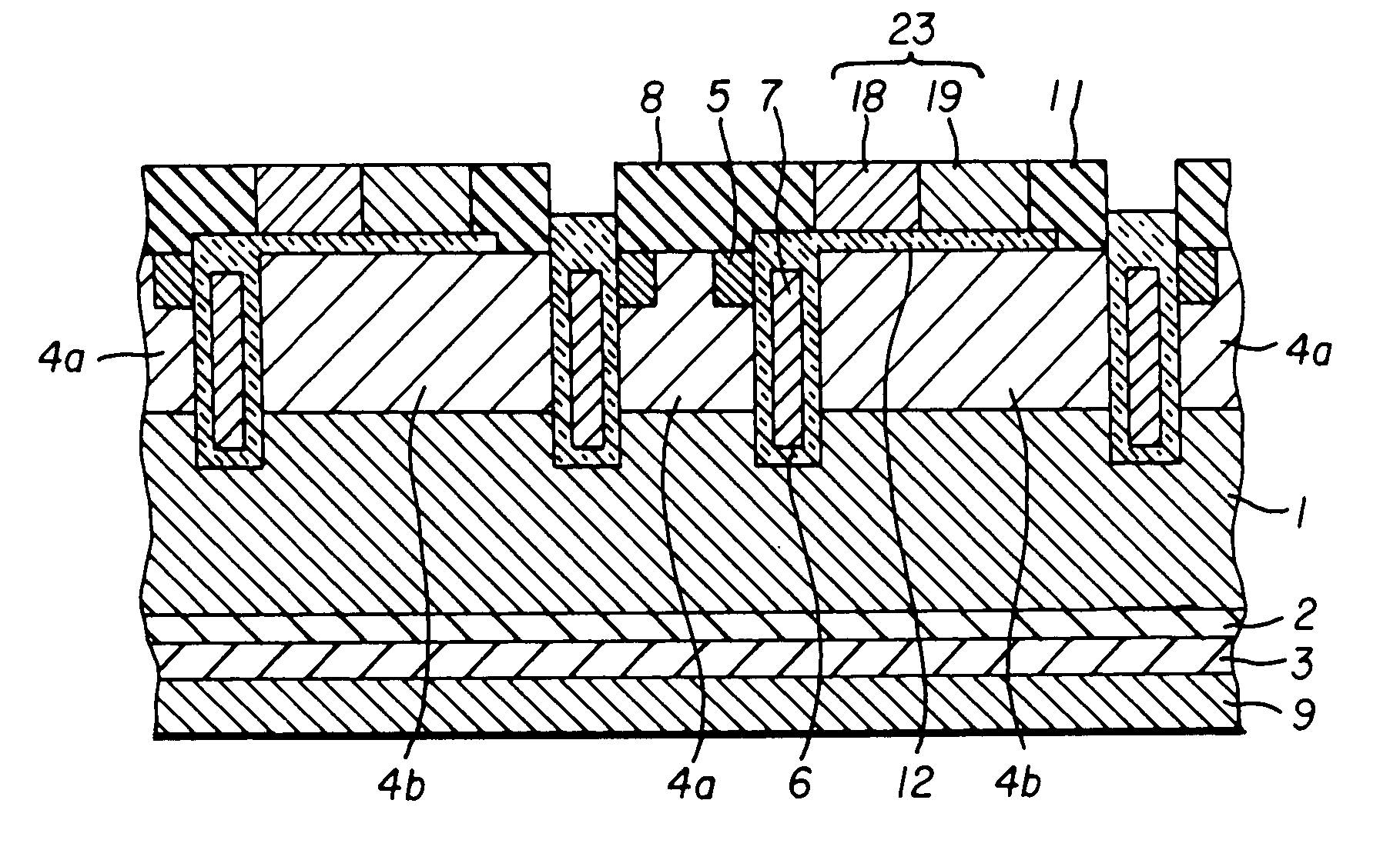
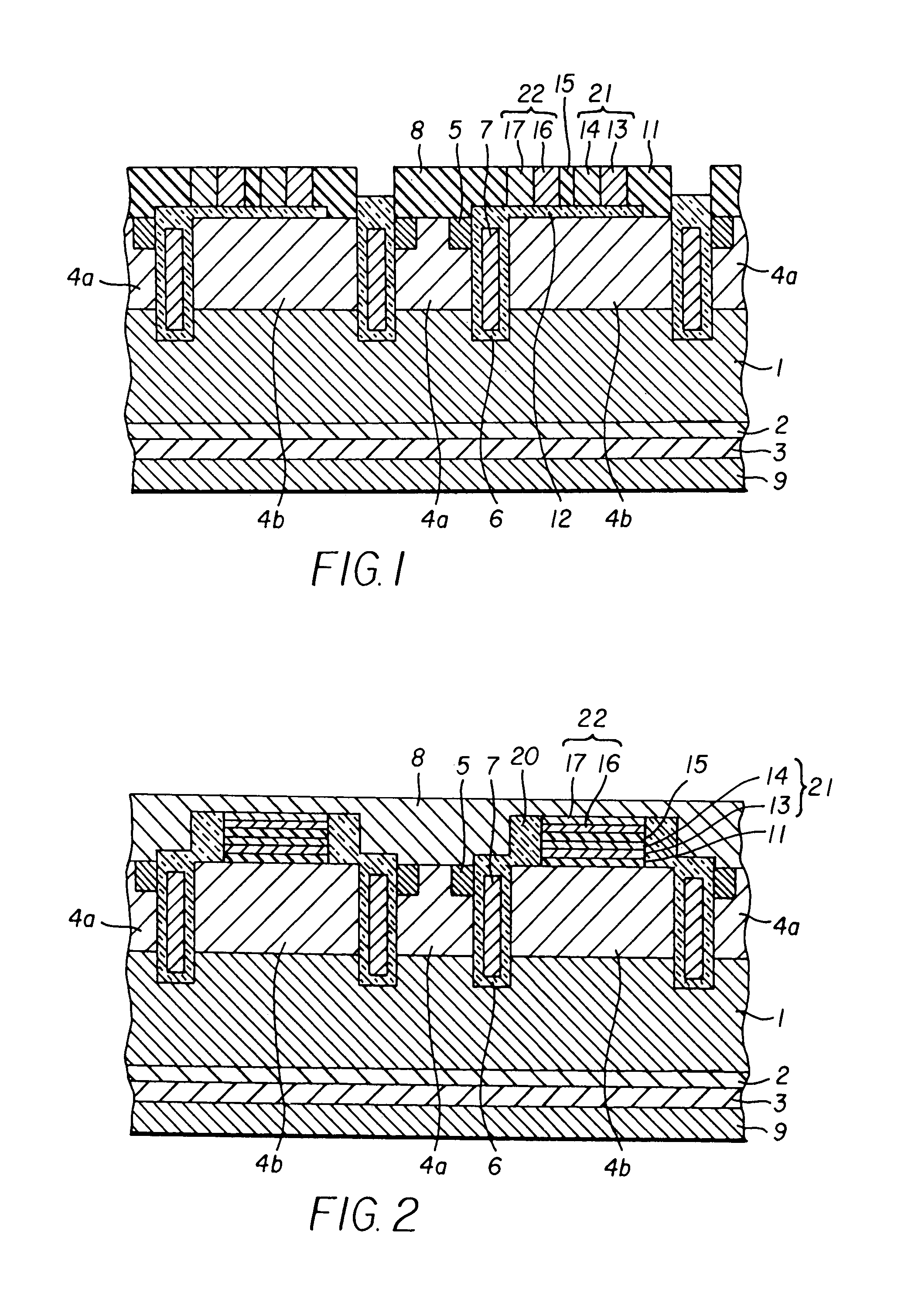
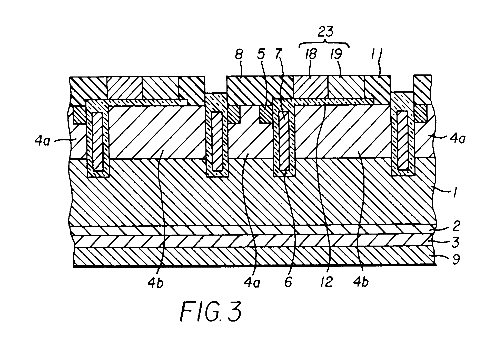
[0035]In the following, explanations will be made in detail about the modes for carrying out the invention with reference to drawings. Here, the explanations will be made about examples in each of which the invention is applied to a field stop IGBT (hereinafter referred to as an “FS-IGBT”) with a structure in which an FZ substrate is used for a semiconductor substrate and, between a drift layer and a collector layer both formed of the substrate, an n-type impurity diffusion layer with a sufficient amount of dose for stopping expansion of an electric field at turning-off is provided as a buffer layer for stopping expansion of the electric field at turning-off.

[0036]FIG. 1 is a vertical cross sectional view showing an example of an FS-IGBT according to the invention. As shown in FIG. 1, on the surface of n-type semiconductor substrate 1, p-type well regions 4a and 4b are formed. A plurality of trenches penetrates through the well regions 4a and 4b from the surface of the substrate to ...


PUM


Abstract

An IGBT having a trench gate structure is disclosed which generates decreased noise at switching and displays superiority in saturation voltage to turn-off loss characteristics (trade-off characteristics). In a part of a region on an emitter side surface interposed between trench gates, a sub well region is provided, which is connected to an emitter electrode through diodes. When the IGBT is in a turned-on state, the diodes are brought into a non-conduction state to isolate the sub well region from the emitter electrode, by which carriers are accumulated. When the IGBT is in a turned-off state, the diodes are brought into a conduction state to electrically connect the sub well region to the emitter electrode, by which carriers are discharged at a high speed. In an early stage of turning-on of the IGBT, capacitance of a portion of the gate facing the sub well region is converted to gate-emitter capacitance to thereby reduce gate-collector capacitance, by which electromagnetic noise at switching is reduced.

Description

[0001]This application claims priority from Japanese application JP PA 2003-129243, filed on May 7, 2003, the contents of which are incorporated by reference herein in their entirety.BACKGROUND OF THE INVENTION[0002]A. Field of the Invention[0003]The present invention relates to an insulated gate bipolar transistor, and more particularly to an insulated gate bipolar transistor having a trench structure in which a gate electrode is buried in a trench formed in a semiconductor substrate with a gate insulator film interposed between.[0004]B. Description of the Related Art[0005]In recent years, under the leadership of Europe and North America, restrictions have been placed on electromagnetic noise generated from semiconductor apparatus provided with power semiconductor devices. It is known that the electromagnetic noise is generated due to variation in a voltage V with respect to time t (hereinafter represented as dV / dt) or variation in a current I with respect to time t (hereinafter re...

Claims


Application Information

Patent Timeline
Patent Type & Authority Patents(United States)
IPC IPC(8): H01L29/73H01L21/76H01L29/78H01L27/04H01L29/417H01L29/739
CPCH01L29/7397H01L29/41741
Inventor YOSHIKAWA, KOHUENO, KATSUNORIKANEMARU, HIROSHI
Owner FUJI ELECTRIC HLDG CO LTD
Why Eureka
Try Eureka