Switchable power domains for 1.2v and 3.3v pad voltages

a technology of switchable power domain and pad voltage, applied in the field of communication systems, can solve the problems of incompatibility between binary levels that each can produce and recognize, and transistors operating at the lower supply voltage. likely to break down and be destroyed

Inactive Publication Date: 2006-08-29
AVAGO TECH INT SALES PTE LTD
View PDF3 Cites 26 Cited by
  • Summary
  • Abstract
  • Description
  • Claims
  • Application Information

AI Technical Summary

Benefits of technology

[0023]The third supply voltage generated internally is chosen so that it does not damage devises comprising the core of the first circuit. Selecting the first supply mode further includes forcing the first supply voltage onto a mode select pin. The method also includes selecting the second supply mode by forcing the second supply voltage onto the mode select pin, and voltage dividing the second supply voltage to obtain the internal supply voltage.

Problems solved by technology

It is not, however, a simple matter to render circuits electrically compatible that must communicate with one another when operating at different supply voltages.
The very fact that the supply voltages are different makes it likely that, without more, the binary levels that each can produce and recognize will be incompatible.
If this voltage is fed into transistors operating at 1.5 volts on the second circuit (or chip), the transistors operating at the lower supply voltage will likely break down and are destroyed.
Unfortunately, the benefits obtained by using a lower supply voltage core are not achieved when meeting the higher voltage interface standard.

Method used


Image

  • Switchable power domains for 1.2v and 3.3v pad voltages
  • Switchable power domains for 1.2v and 3.3v pad voltages
  • Switchable power domains for 1.2v and 3.3v pad voltages

Examples


Embodiment Construction

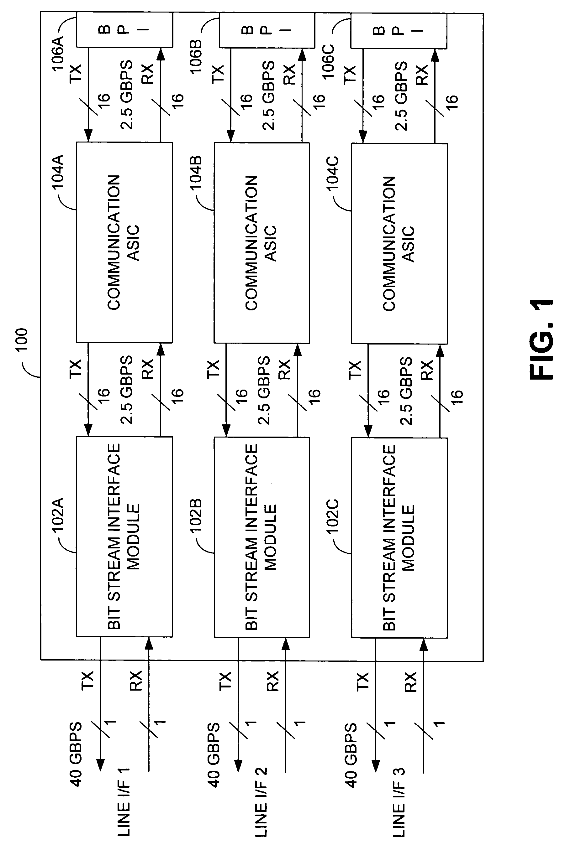
[0039]FIG. 1 is a block diagram illustrating a Printed Circuit Board (PCB) that has mounted thereon a plurality of Bit Stream Interface Module (BSIMs) integrated circuits constructed according to the present invention. As shown in FIG. 1, the PCB 100 includes BSIMs 102A, 102B and 102C. The PCB 100 also includes mounted thereon communication Application Specific Integrated Circuits (ASIC) 104A, 104B, and 104C. The PCB 100 is mounted within a housing that services switching requirements within a particular location or geographic area. Each of the BSIMs 102A, 102B, and 102C couples to a high-speed media such as an optical fiber via a respective media interface and supports the OC-768 or the SEC-768 standard at such media interface. On the second side of the BSIMs 102A through 102C, the SFI-5 interface standard is supported for communication between the BSIM 102A, 102B, and 102C and the ASICs chips 104A, 104B, and 104C. Communication ASICs 104A through 104C may communicate with other PC...


PUM


Abstract

An integrated circuit includes a core circuit and a buffer circuit. The buffer circuit includes a plurality of input buffers and a plurality of output buffers that service a plurality of voltage domains on a single set of input / output lines. These voltage domains are controllable to service multiple voltage levels, consistent with various interface standards. In one construction, the core circuit operates at 1.2 volts and the buffer circuit supports both a 1.2 volts interface standard and a 3.3 volts interface standard.

Description

CROSS REFERENCES TO RELATED APPLICATIONS[0001]This application is a continuation of U.S. Ser. No. 10 / 448,640 filed May 30, 2003, now issued as U.S. Pat. No. 6,943,587 which claims priority to U.S. Provisional Application Ser. No. 60 / 403,455, filed Aug. 12, 2002, which is incorporated herein by reference in its entirety for all purposes.BACKGROUND OF THE INVENTION[0002]1. Technical Field of the Invention[0003]The present invention relates generally to communication systems, and more particularly to the interface between high-speed serial bit stream communication circuits having different power supply voltages.[0004]2. Description of Related Art[0005]The structure and operation of communication systems is generally well known. Communication systems support the transfer of information from one location to another location. Early examples of communication systems included the telegraph and the public switch telephone network (PSTN). When initially constructed, the PSTN was a circuit swi...

Claims


Application Information

Patent Timeline
Patent Type & Authority Patents(United States)
IPC IPC(8): H03K19/0175H03K19/0185H04L7/00
CPCH03K19/018585H04L7/0008
Inventor JOSHI, SRIDEVI R.YIN, GUANGMINGNEJAD, MOHAMMADSCHOCH, DANIEL
Owner AVAGO TECH INT SALES PTE LTD
Why Eureka
Try Eureka