Electrooptic device, driving method therefor, electronic device, and projection display device

a technology of electronic devices and driving methods, applied in the direction of optics, identification means, instruments, etc., can solve the problems of irregular charges inevitably remaining everywhere inside the electrooptic device, the above-described problem is more pronounced, and the electrooptic device is prone to irregular charges, etc., to achieve high-quality image display

Active Publication Date: 2006-08-29
138 EAST LCD ADVANCEMENTS LTD
View PDF22 Cites 26 Cited by
  • Summary
  • Abstract
  • Description
  • Claims
  • Application Information

AI Technical Summary

Benefits of technology

[0009]The present invention has been made in view of the above problem, and an object of the present invention is to provide an electrooptic device that can perform high-quality image display so that an afterimage or the like due to charges accumulated therein is not formed on an image, a driving method therefor, an electronic device, and a projection display device.

Problems solved by technology

However, conventional electrooptic devices have the following problem.
Therefore, irregular charges inevitably remain everywhere inside the electrooptic device during operation of the electrooptic device.
In a case in which the electrooptic device has storage capacitors, the above-described problem tends to be more pronounced.
However, such provision of storage capacitors is equal to the addition of new places in which charges are accumulated inside the electrooptic device, and the above problem appears more pronouncedly.
In addition, in recent electrooptic devices, the cell gap between the TFT array substrate and the counter substrate is further reduced, and the structure of the storage capacitors is complicated in order to achieve size reduction and high definition.
Consequently, it is more difficult to remove accumulated charges, and there is a greater fear that the above problem will arise.

Method used


Image

  • Electrooptic device, driving method therefor, electronic device, and projection display device
  • Electrooptic device, driving method therefor, electronic device, and projection display device
  • Electrooptic device, driving method therefor, electronic device, and projection display device

Examples


first embodiment

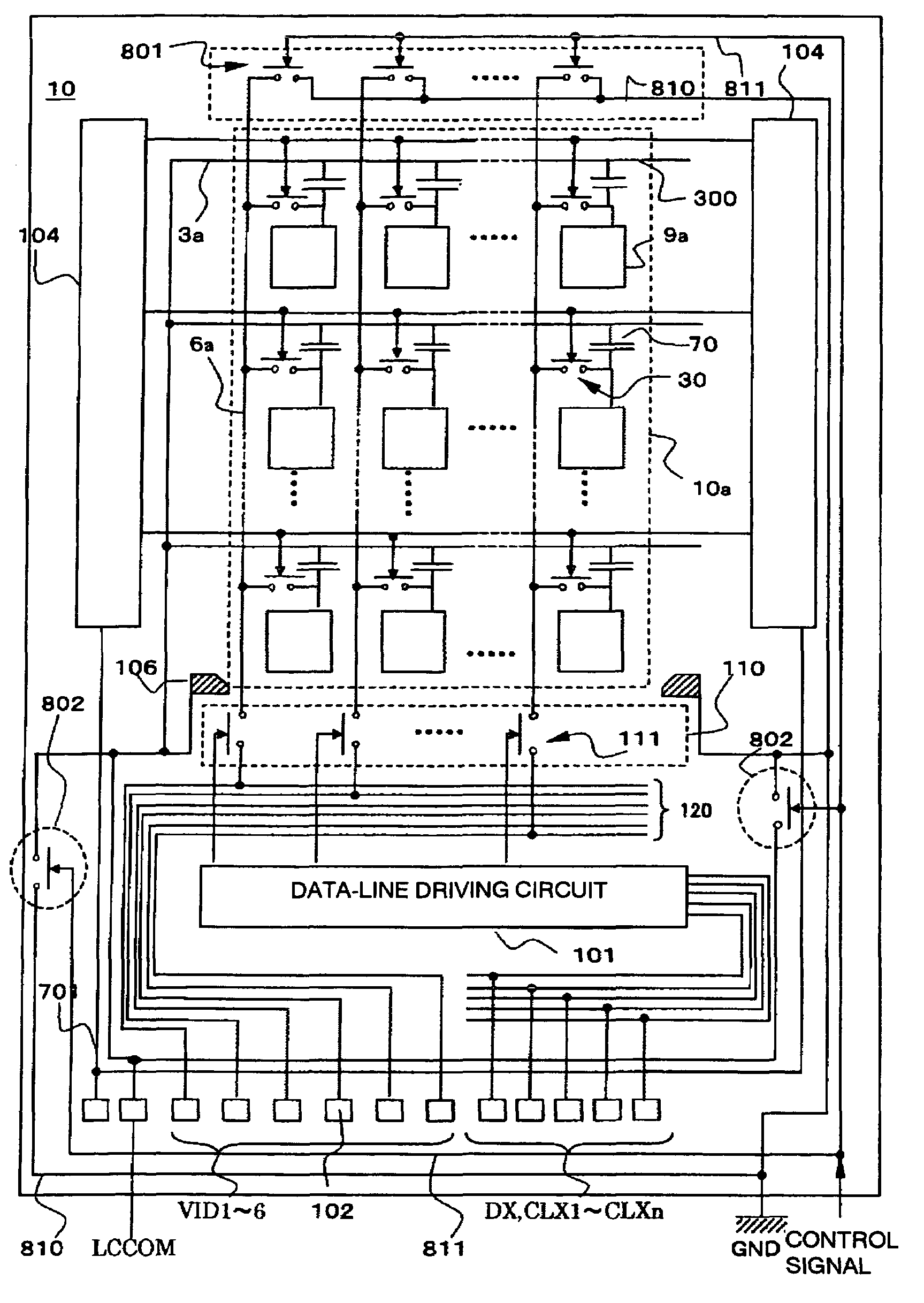
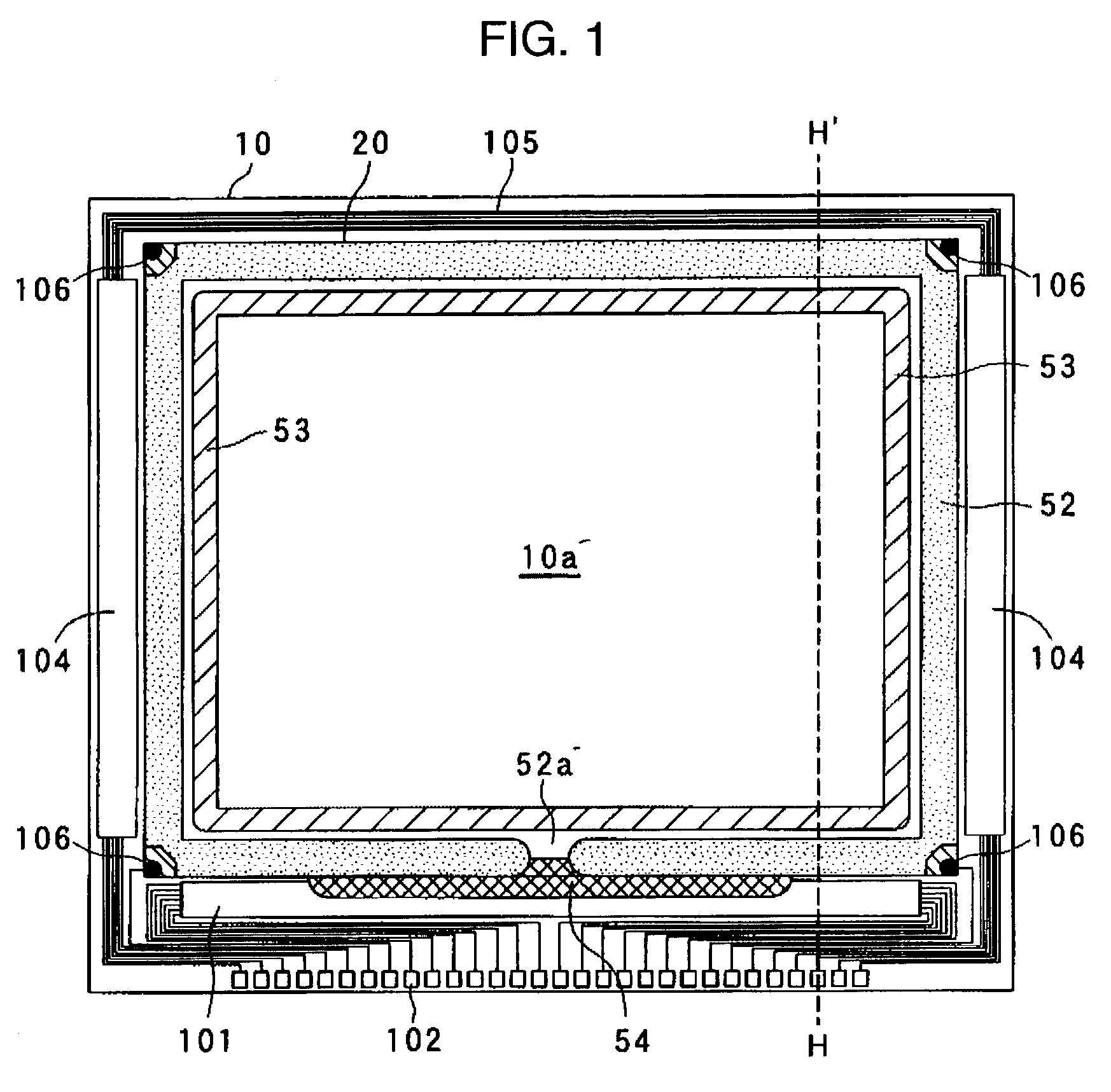
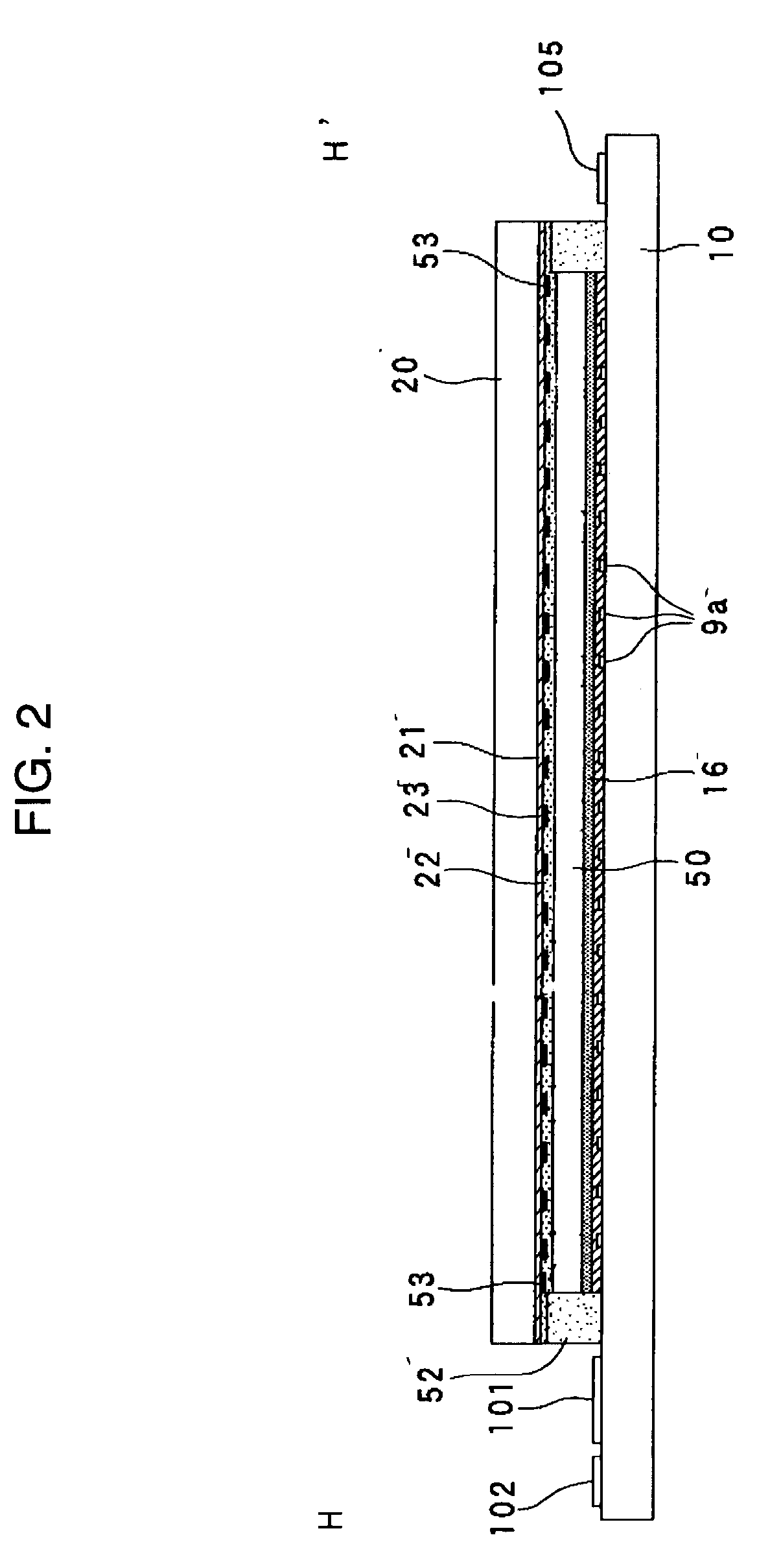
[0070]An electrooptic device will be first described with reference to FIGS. 1 to 3. FIG. 1 is a plan view of a TFT array substrate and components formed thereon, as viewed from the side of a counter substrate 20, and FIG. 2 is a cross-sectional view, taken along line H–H′ in FIG. 1. FIG. 3 is a plan view schematically showing the configurations of circuits, such as pixel electrodes, scanning lines, and data lines, formed on the TFT array substrate, and manners of connections between the circuits and various peripheral circuits.

[0071]First, the electrooptic device of the first embodiment is generally shaped by placing a TFT array substrate 10 and a counter substrate 20 opposed to each other, as shown in FIGS. 1 and 2. A liquid crystal layer 50 is sealed between the TFT array substrate 10 and the counter substrate 20, and the TFT array substrate 10 and the counter substrate 20 are bonded together with a sealing material 52 provided in a sealing region around an image display region ...

second embodiment

[0109]In the second embodiment, first, operations of turning off a power switch and of cutting off external input signals to light valves 100R, 100G, and 100B are identically performed in Steps S11 and S12 in FIG. 7.

[0110]In the second embodiment, in particular, an image signal representing image display of the single-color, that is, a single-color signal is supplied to pixel electrodes 9a after the above operations (Step S23). This operation is performed through data lines 6a by the actions of a control circuit 1012, display-information output source 1000, display-information processing circuit 1002, image signal line 120, a sample-and-hold circuit 110, a data-line driving circuit 101, and the like. A specific form of the single-color signal is determined by the driving mode of the light valves 100R, 100G, and 100B. In other words, in a normally white mode in which the alignment state of liquid crystal molecules that constitute a liquid crystal layer 50 changes in a direction to re...


PUM

PropertyMeasurementUnit
diameteraaaaaaaaaa
thicknessaaaaaaaaaa
timeaaaaaaaaaa

Abstract

The invention provides an electrooptic device that can include a first substrate on which pixel electrodes, first thin film transistors electrically connected to the pixel electrodes, and scanning lines and data lines electrically connected to the first thin film transistors are formed, a second substrate opposing the first substrate and having a common electrode, and an electrooptic substance held between the first substrate and the second substrate. The electrooptical device can further include a switching element for discharging in capacitors constituted by the pixel electrodes on the first substrate, the electrooptic substance, and the common electrode on the second substrate. The invention makes it possible to remove charges from inside the electrooptic device.

Description

BACKGROUND OF THE INVENTION[0001]1. Field of Invention[0002]The present invention relates to technical fields of electrooptic devices and electronic devices. More particularly, the invention relates to technical fields of an electrooptic device having various capacitors in which charges are accumulated, a driving method therefor, an electronic device, and a projection display device.[0003]2. Description of Related Art[0004]Currently, electrooptic devices are known which can be driven by a so-called active matrix driving method by having pixel electrodes arranged in a matrix, thin film transistors (TFT) connected to the pixel electrodes, scanning lines and data lines provided in parallel in rows and columns, and the like. Such electrooptic devices can further include a TFT array substrate on which the TFTs, the pixel electrodes, and the like described above are formed, a counter substrate opposing the TFT array substrate and having a common electrode, and an electrooptic substance, s...

Claims


Application Information

Patent Timeline
Patent Type & Authority Patents(United States)
IPC IPC(8): G09G3/36G02F1/133G02F1/13G02F1/1362G02F1/1368G09F9/30G09G3/20H01L21/336H01L29/786
CPCG09G3/3655G02F1/136213G09G2330/022G09G2310/0245G09G2300/0876G02F1/133
Inventor INOUE, KENHIRASE, TOSHIYUKIUCHIYAMA, SADASUMI
Owner 138 EAST LCD ADVANCEMENTS LTD
Why Eureka
Try Eureka