Plasma display panel and manufacturing method therefor

a technology of display panel and plasma, which is applied in the manufacture of electrode systems, cold cathode, electric discharge tube/lamps, etc., can solve the problems of high cost of pdps, decreased discharge probability, and increased possibility of discharge, so as to reduce the occurrence of black noise, increase the discharge probability, and reduce the firing voltage

Inactive Publication Date: 2006-09-05
PANASONIC CORP
View PDF12 Cites 14 Cited by
  • Summary
  • Abstract
  • Description
  • Claims
  • Application Information

AI Technical Summary

Benefits of technology

[0014]In view of the stated problems, the object of the present invention is to provide a PDP, and a manufacturing method therefor, that is able to increase discharge probability by reducing firing voltage Vf without using expensive, highly voltage-resistant transistor and driver ICs, and that has a protective layer that is able to reduce the occurrence of black noise in which cells that should be illuminated are not illuminated, by maintaining wall charge retention.

Problems solved by technology

This is one factor that contributes to the high cost of PDPs.
When the driving time is shortened, the discharge probability decreases, and therefore the possibility increases of discharge, such as address discharge, not being performed reliably.
However, if this method is employed, the number of data drivers required is twice that of an ordinary PDP and wiring becomes complicated.
These factors contribute to high costs and low yield in manufacturing PDPs.
However, the conventional techniques are problematic in that they are unable to both reduce the firing voltage Vf sufficiently and solve display instability called “black noise”.

Method used


Image

  • Plasma display panel and manufacturing method therefor
  • Plasma display panel and manufacturing method therefor
  • Plasma display panel and manufacturing method therefor

Examples


first embodiment

[0026]1. First Embodiment

[0027]1-1. Structure of the PDP

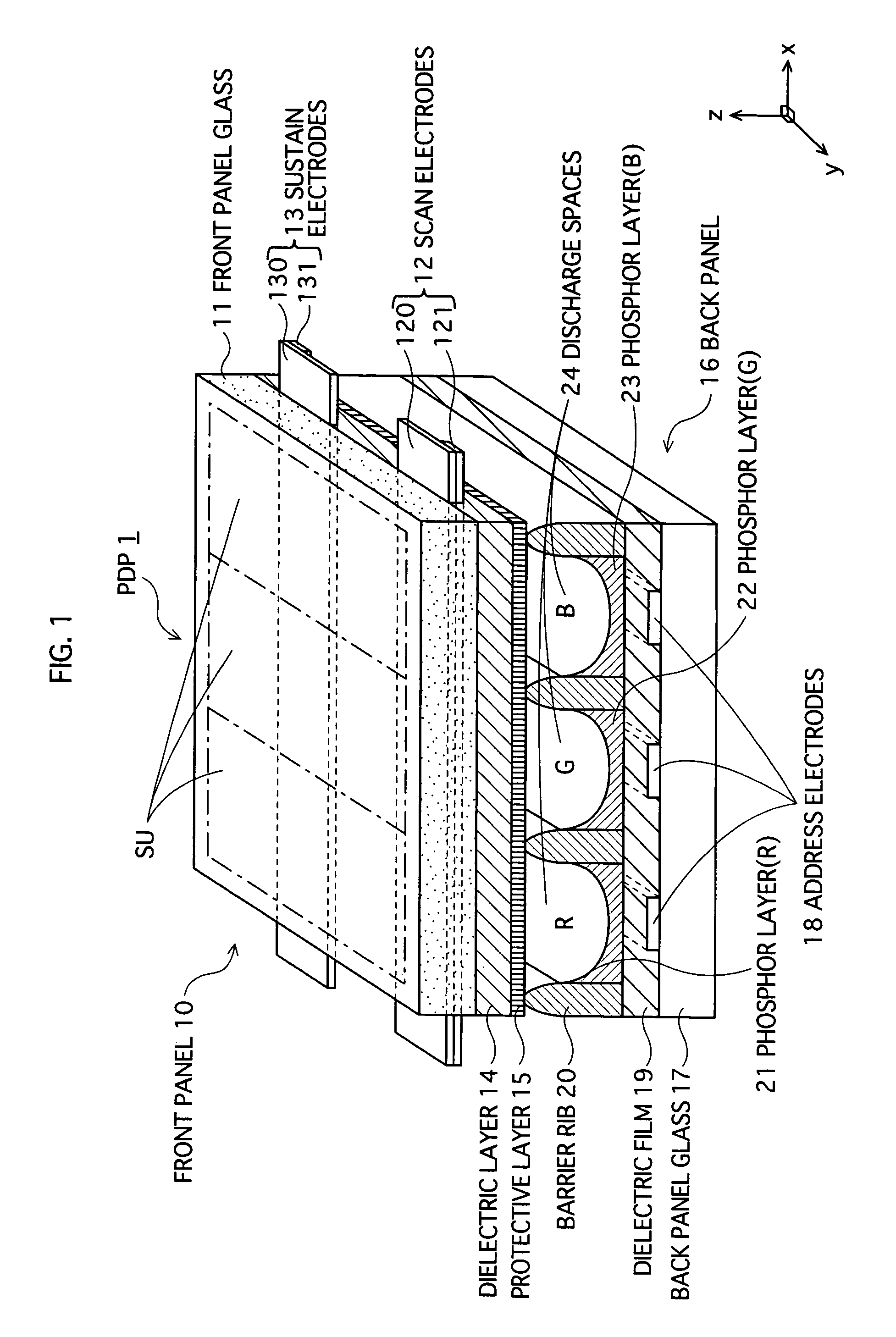
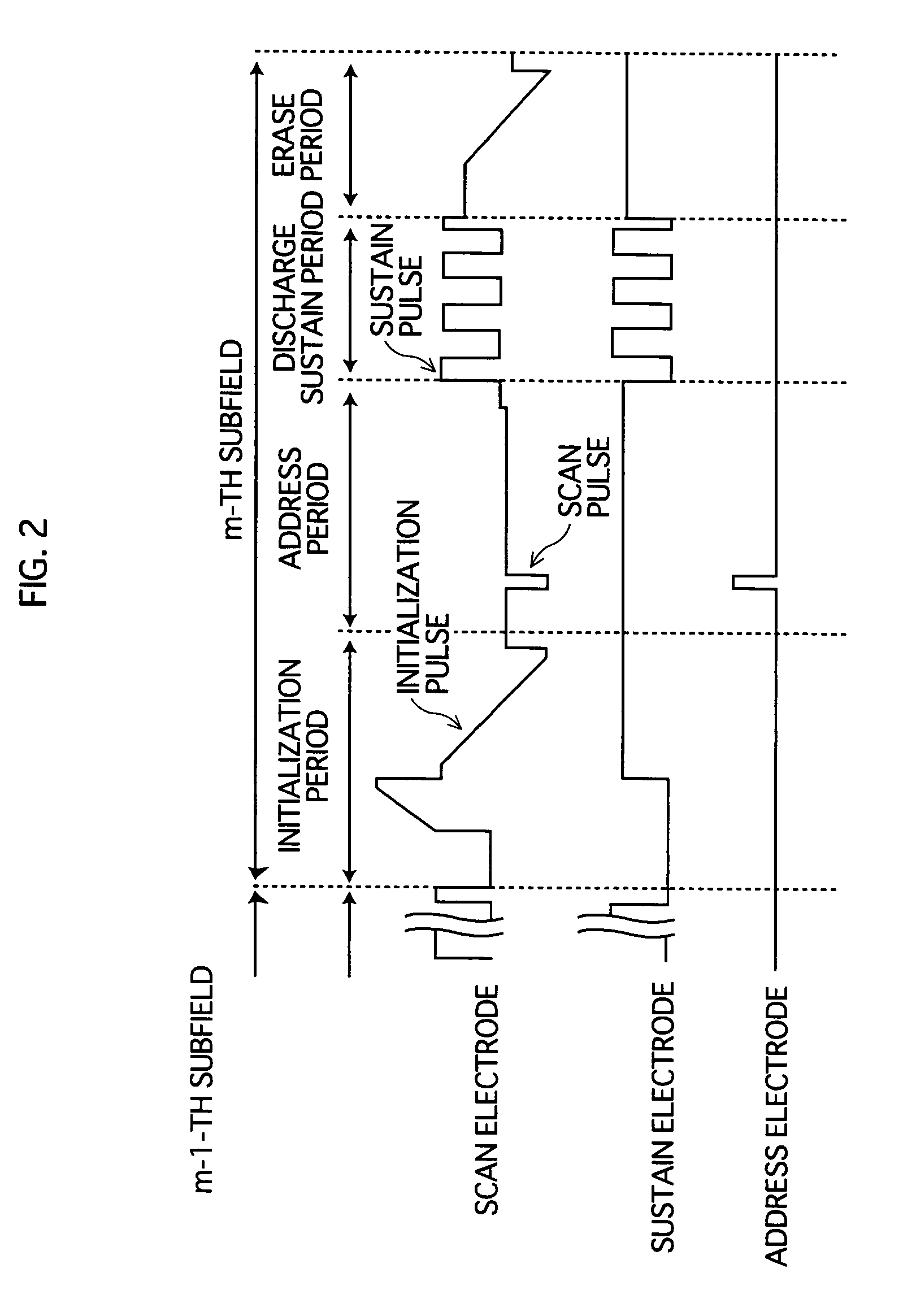
[0028]FIG. 1 is a cross-sectional perspective drawing partially showing relevant structure of an AC PDP 1 of the first embodiment of the present invention. In FIG. 1, a z direction corresponds to a thickness direction of the PDP 1, and an xy plane corresponds to a plane parallel to a panel surface of the PDP 1. Here, as one example, the PDP 1 is a 42-inch class NTSC PDP. However, the present invention may be applied to other specifications such as XGA (extended graphic array) and SXGA (super extended graphics array), and other sizes.

[0029]As shown in FIG. 1, the structure of the PDP 1 can be divided broadly into a front panel 10 and a back panel 16, which are arranged with their respective main surfaces opposing each other.

[0030]The front panel 10 includes a sheet of front panel glass 11 that has a plurality of pairs of display electrodes 12 and 13 formed on one main surface thereof (each pair being composed of a scan electrode...

second embodiment

[0115]3. Second Embodiment

[0116]3-1. Structure of the PDP

[0117]The overall structure of the PDP 1 of the second embodiment is almost the same as that of the first embodiment, and is characterized by the protective layer 15.

[0118]Specifically, the main characteristic of the PDP 1 of the second embodiment is that the MgO crystals that make up the protective layer 15 are doped with a metal element Cr from the surface of the protective layer 15 extending for a depth of at least 100 nm, with a density of concentration of 1E18 / cm3. In addition, the MgO crystals have a structure that includes an oxygen vacancy defect.

[0119]According to this structure, the first energy level is created in the forbidden band of the MgO of the protective layer 15 by the oxygen vacancy defect, and the second energy level is created in the forbidden band by the Cr. This achieves substantially the same effects as the first embodiment.

[0120]Additionally, in the second embodiment the Cr used as a dopant works as l...

third embodiment

[0132]4. Third Embodiment

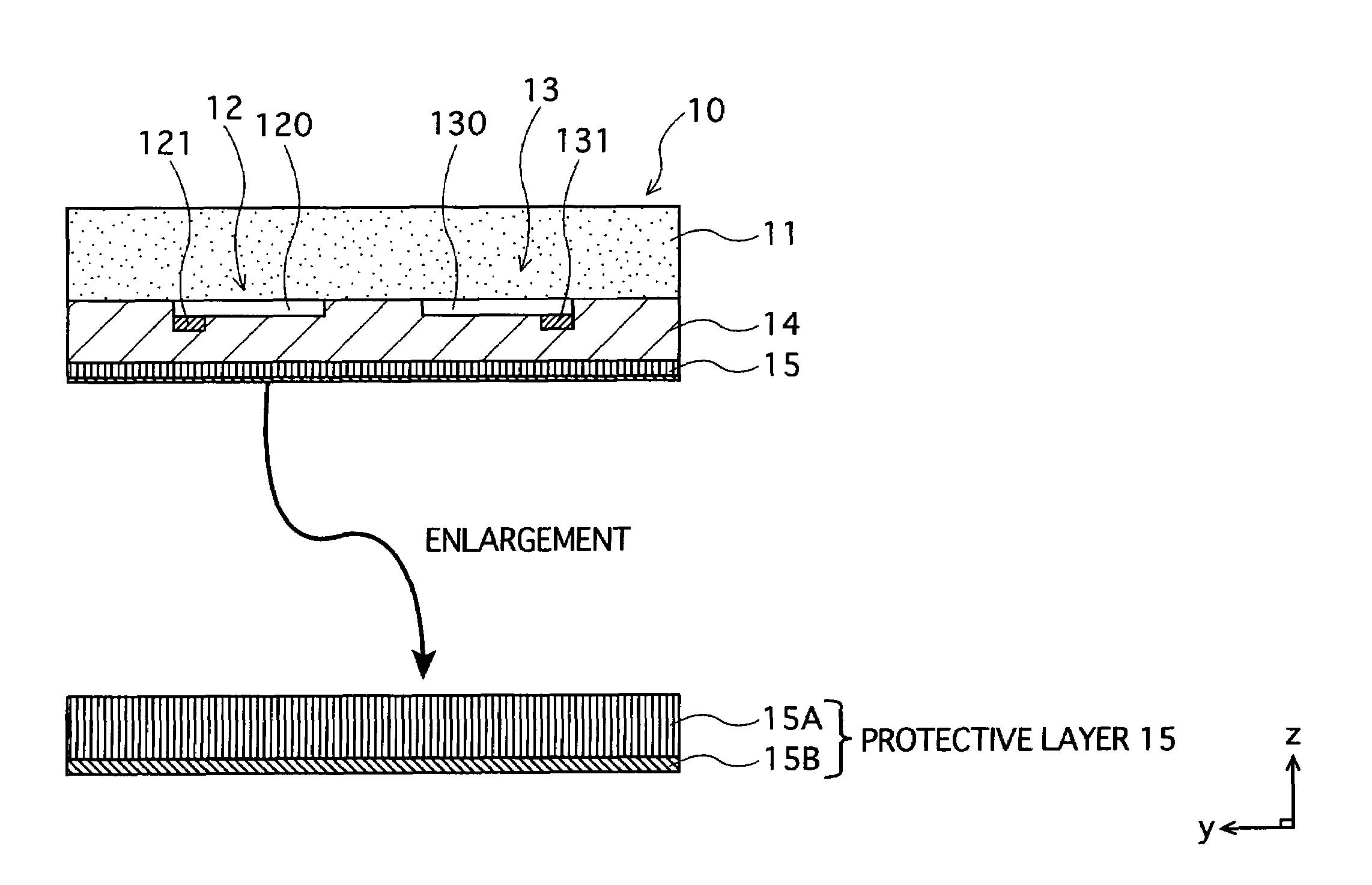
[0133]FIG. 5 is a partial cross-sectional diagram of the structure of the protective layer 15 of the PDP 1 of the third embodiment. As shown in FIG. 5, the protective layer 15 of the third embodiment is composed of two layers 15A and 15B, of which the protective layer 15A, which is made of MgO that is approximately 100 nm thick, is doped at the surface with Cr and has an oxygen vacancy defect. In this structure also, the oxygen vacancy defect creates the first energy level and the Cr creates the second energy level. In this way, in the present invention, the protective layer 15 is not limited to having uniform qualities in the thickness direction. The effects of the present invention can be obtained as long as first and second energy levels are created at least in a vicinity of the surface of the protective layer 15. The thickness of approximately 100 nm is selected so as to be greater than the thickness thought to be required considering wear of the protect...


PUM


Abstract

A plasma display panel is composed of a first substrate and a second substrate facing each other via a discharge space and sealed together. A protective layer on the first substrate is composed principally of magnesium oxide, includes a substance or structure that creates a first energy level in an area of a forbidden band, the area being in a vicinity of a conduction band, and includes a substance or structure that creates a second energy level in another area in the forbidden band, the other area being in a vicinity of a valence band. During driving the second energy level is occupied by electrons, and few electrons exist in the first energy level, or electrons can easily occupy the first energy level due to a minus charge state, and MgO insultaive resistance is not lowered. This maintains wall charge retention and reduces discharge irregularities and firing voltage Vf.

Description

BACKGROUND OF THE INVENTION[0001](1) Field of the Invention[0002]The present invention relates to a plasma display panel and a manufacturing method therefor, and in particular to a method for forming a magnesium oxide protective layer that covers a dielectric layer.[0003](2) Description of Related Art[0004]A plasma display panel (hereinafter referred to as a “PDP”) is a gas discharge panel in which images are displayed according to phosphor that emits light by being excited by ultraviolet rays generated by gas discharge. PDPs are divided into two types: alternating current (AC) and direct current (DC), depending of the method used to discharge. AC PDPs are the more common type due to their superiority over DC PDPs in terms of luminance, luminous efficiency, and lifespan.[0005]An AC PDP has the following structure. A plurality of electrodes (display electrodes and address electrodes) are arranged on each of two thin sheets of panel glass. The exposed parts of the surface of each shee...

Claims


Application Information

Patent Timeline
Patent Type & Authority Patents(United States)
IPC IPC(8): H01J17/49H01J9/02
CPCH01J9/02H01J11/40H01J11/12
Inventor NISHITANI, MIKIHIKOMORITA, YUKIHIROKITAGAWA, MASATOSHITERAUCHI, MASAHARU
Owner PANASONIC CORP
Why Eureka
Try Eureka