Image pickup device capable of adjusting the overflow level of the sensor based on the read out mode

a pickup device and sensor technology, applied in the field of image pickup devices, can solve the problems of deteriorating picture quality, finite saturated level, horizontal streak noise along the horizontal line,

Inactive Publication Date: 2006-09-05
OLYMPUS CORP
View PDF15 Cites 18 Cited by
  • Summary
  • Abstract
  • Description
  • Claims
  • Application Information

AI Technical Summary

Benefits of technology

[0012]In accordance with the purpose of the invention, as embodied and broadly described, the invention is directed to an image pick-up device which prevents a horizontal streak noise from being occurred in the pixel addition.

Problems solved by technology

When a high-luminance subject is imaged, however, n-addition driving may cause a white-striped pseudo signal (a phenomenon similar to blooming or a smear, in this specification, referred to as horizontal streak noise) in the horizontal direction, which will possibly deteriorate the picture quality.
Actually, however, the saturated level is finite.
In some actual CCDs, unsatisfactory excess charge measures have been taken for the horizontal transfer path, permitting the excess charges to overflow into the regions adjacent to the horizontal transfer path, which causes horizontal streak noise along the horizontal lines.

Method used


Image

  • Image pickup device capable of adjusting the overflow level of the sensor based on the read out mode
  • Image pickup device capable of adjusting the overflow level of the sensor based on the read out mode
  • Image pickup device capable of adjusting the overflow level of the sensor based on the read out mode

Examples


first embodiment

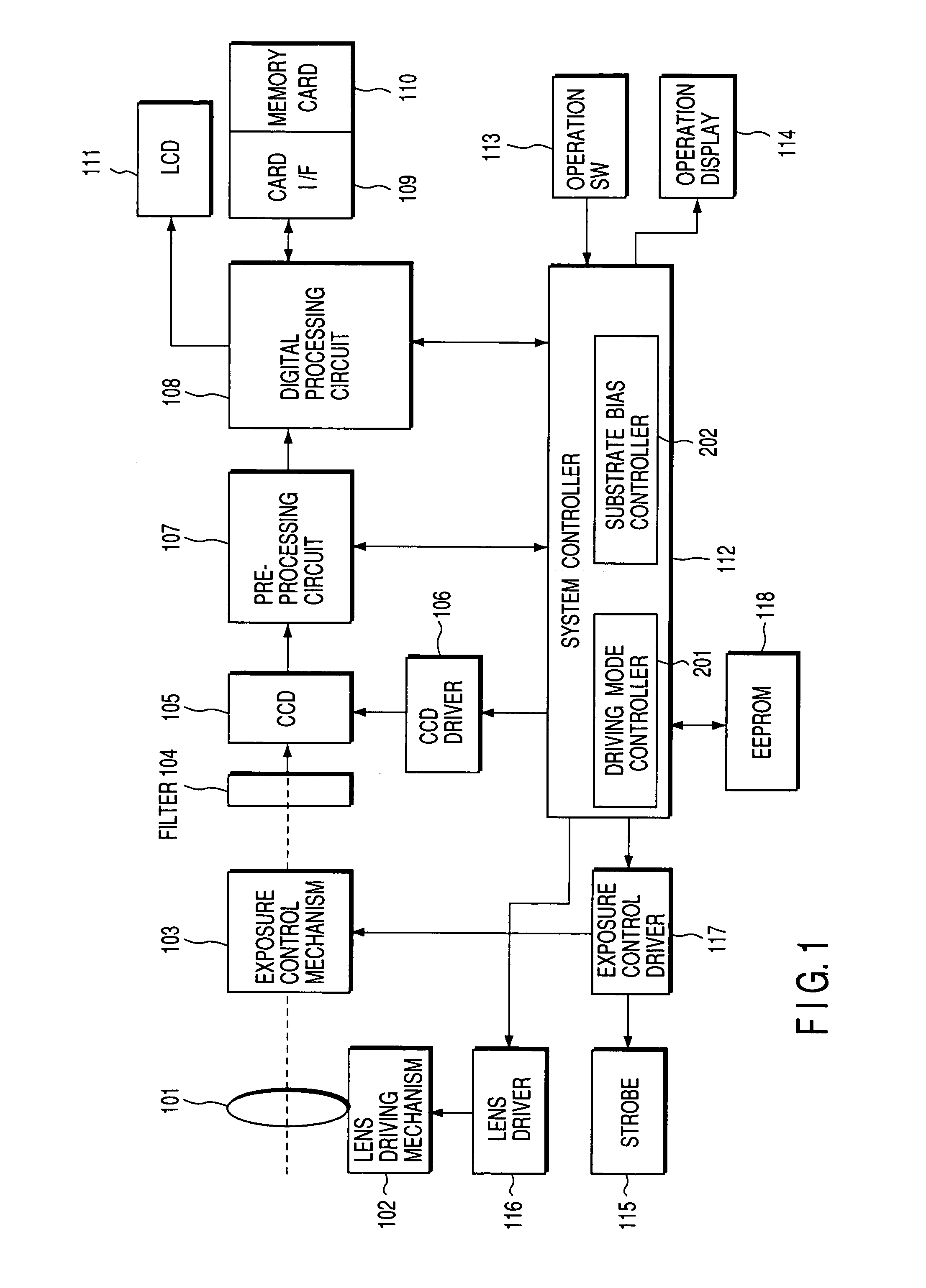
[0031]FIG. 1 is a block diagram showing the first embodiment of the present invention. Light passed through a lens system 101 passes through an exposure control mechanism 103 (the stop of the lens system 101) and an optical filter 104 for cutting out high-frequency components and infrared components and is projected (or focused) on to a CCD 105. The CCD 105 has a color filter where a plurality of color components are arranged in a mosaic, pixel by pixel, at the image forming surface of the CCD. The output of the CCD 105 is inputted via a preprocessing circuit 107 including an A / D converter to a digital processing circuit 108 for carrying out a color signal generating process, a matrix conversion process, and various other digital processes. The color signal generated by the digital processing circuit 108 is displayed on an LCD display unit 111, acting as a viewfinder. A card interface 109 stores the color signal in a memory card 110 incorporating a nonvolatile memory which is a stor...

second embodiment

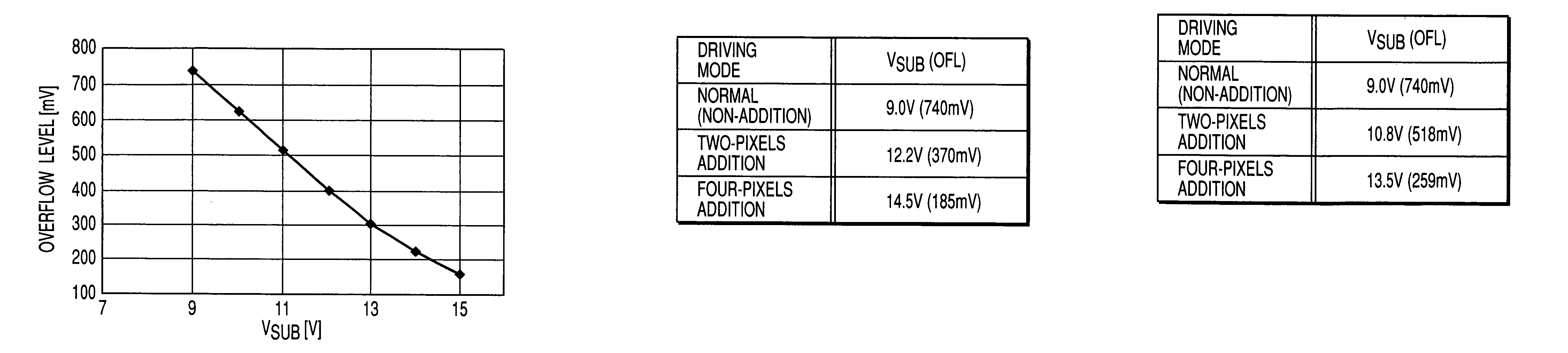
[0068]When the substrate bias voltage VSUB is varied, the color balance in the n-addition mode may differ from that in the non-addition mode. The sensitivity characteristic of the charge accumulating portion depends on the substrate bias voltage VSUB. Since the dependence is greater on the long wavelength side, the spectral characteristic also depends on the substrate bias voltage VSUB. This means that the R, G, B relative sensitivity of the CCD varies.

[0069]FIG. 8, where the value on the abscissa is wavelength in nm, shows a spectral sensitivity characteristic of the non-addition mode (solid line) and n-addition mode (broken line). In the spectral characteristic, B increases and R decreases in the n-addition mode (when the substrate bias voltage VSUB is raised), with G as a reference.

[0070]Traditionally, although the substrate bias voltage VSUB is subjected to fine adjustment in the camera manufacturing process, it is used almost in a fixed manner after the fine adjustment. In this...

third embodiment

[0087]In the second embodiment, the spectral characteristic is corrected on the basis of the variation characteristic of the spectral sensitivity with respect to a change in the substrate bias voltage shown in FIG. 10. FIG. 10 shows the relative magnitude of the B and R signals in the form of spectral sensitivity, using G as a reference (G=100 invariable). Therefore, when the absolute sensitivity (luminance sensitivity) is invariable in the n-addition driving with regards to the non-addition driving, the second embodiment applies to n-addition driving as it is. Actually, however, not only spectral sensitivity characteristics but also absolute sensitivity characteristics in n-addition driving may differ from those in non-addition driving. Hereinafter, a third embodiment of the present invention coping with such a change in the absolute sensitivity will be explained. Since the block diagram showing the configuration of the device is the same as that of FIG. 9, it will be omitted.

[0088...


PUM


Abstract

The driving device of a solid-state imaging device comprises a driving unit for driving the solid-state imaging device in either an addition driving mode in which a plurality of pixels are added and read as a single pixel or a non-addition driving mode, and a substrate bias voltage supply for applying a bias voltage to the substrate of the solid-state imaging device according to the driving mode. The substrate bias voltage is set according to the number of pixels added in the addition driving mode so that the overflow level of the charge accumulating portion may be lower in the addition driving mode than in the normal driving mode. This suppresses the input of excess charges to the horizontal transfer path even in the addition driving mode, thereby preventing the generation of horizontal streak noise.

Description

CROSS-REFERENCE TO RELATED APPLICATIONS[0001]This application is based upon and claims the benefit of priority from the prior Japanese Patent Applications No. 2000-69154, filed Mar. 13, 2000 and No. 2000-215103, filed Jul. 14, 2000, the entire contents of which are incorporated herein by reference.BACKGROUND OF THE INVENTION[0002]The present invention relates to an image pickup device using solid-state imaging elements, such as charge-coupled devices (CCDs), and more particularly to a driving method and driving device which perform pixel addition by special driving.[0003]In recent years, various digital cameras using solid-state imaging elements, such as CCDs, have been developed. In a digital camera, the photoelectric conversion portion converts an image of the subject photoelectrically, thereby producing a pixel signal (charge). The pixel signal is transferred over a transfer path including CCDs and then outputted. To read the pixel signal from the image pickup device, a driving m...

Claims


Application Information

Patent Timeline
Patent Type & Authority Patents(United States)
IPC IPC(8): H04N3/14H01L27/148H04N5/341H04N5/343H04N5/359H04N5/372H04N5/3728
CPCH01L27/14812H01L27/14868H04N5/3728H04N5/343H04N5/3592H01L27/14887H04N25/42H04N25/622H04N25/73
Inventor MORI, KEIICHIYOSHIDA, HIDEAKI
Owner OLYMPUS CORP
Why Eureka
Try Eureka