Method to control artifacts of microstructural fabrication

a microstructure and artifact technology, applied in the direction of instruments, fluid pressure measurement, vacuum gauges, etc., can solve the problems of affecting the desired motion of the components of the device, and affecting the stability of the devi

Active Publication Date: 2006-09-12
NAT TECH & ENG SOLUTIONS OF SANDIA LLC
View PDF113 Cites 16 Cited by
  • Summary
  • Abstract
  • Description
  • Claims
  • Application Information

AI Technical Summary

Problems solved by technology

Gross assembly steps require precision handling, positioning, and bonding of delicate millimeter-scale structures, which are fraught with opportunities for failure.
In particular, when the goal is a micromechanical device, the bonding materials can easily interfere with the desired motion of the components of the device.
Similarly, when the goal is a microfluidic device, the bonding materials can block the flow channels, or prevent microvalves from functioning properly.
Working against the above motivations for direct fabrication of complex microstructures is the difficulty of fabricating such microstructures in their entirety.
As the complexity of a process required for fabrication of a desired silicon microstructure increases, the useful yield of that process falls rapidly toward zero.
Complex fabrication processes are not only susceptible to error, but in many cases can lead to accumulation of residual stress, nonplanarity, and other structural flaws which can render the desired product unusable.
Aspect-ratio-dependent etching effects can result in the need to define and etch narrow features separately from wider features, resulting in an undesirable increase in the complexity of the overall fabrication process.

Method used


Image

  • Method to control artifacts of microstructural fabrication
  • Method to control artifacts of microstructural fabrication
  • Method to control artifacts of microstructural fabrication

Examples


Embodiment Construction

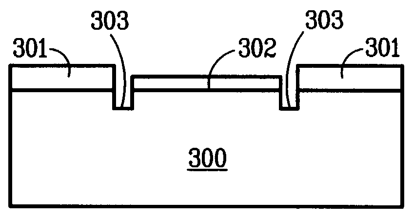
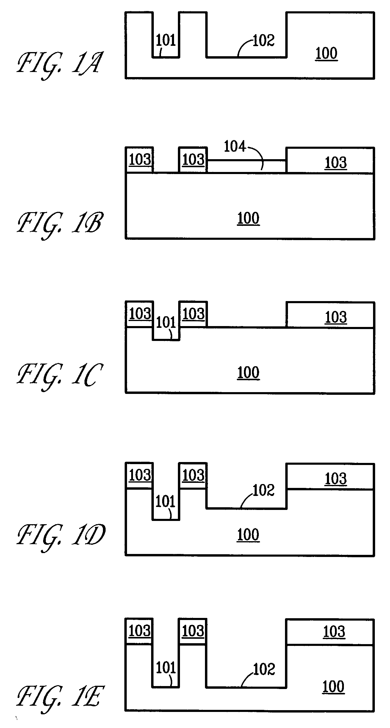
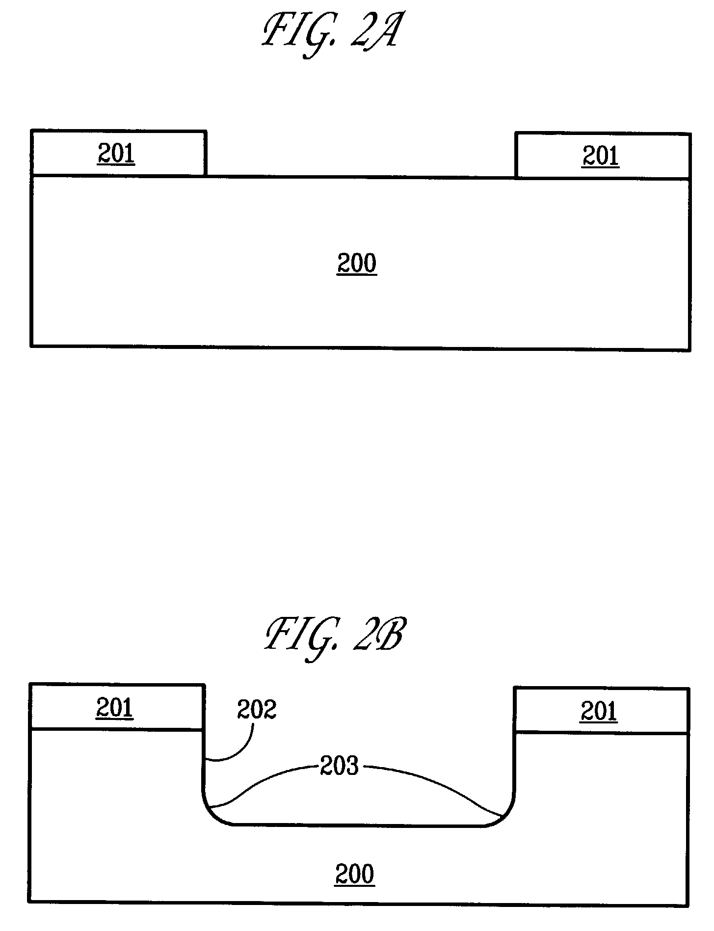
[0015]FIG. 1 illustrates the use of an etching delay layer in the fabrication of microstructures having features with a range of pattern shapes. Specifically, FIG. 1a shows the target microstructure. A narrow groove 101 and a wide groove 102 are to be fabricated in a substrate 100. Grooves 101 and 102 are to have the same nominal depth below the original surface of the substrate.

[0016]FIG. 1b shows the structure immediately prior to the start of the etching process. Mask layer 103 is deposited atop substrate 100. Mask layer 103 can be either a conventional photoresist layer or a thin film hard mask (metal or dielectric) layer, and is patterned so as to define etching windows for narrow groove 101 and wide groove 102.

[0017]Etching delay layer 104 is deposited on substrate 100 within the etching window for wide groove 102. Delay of the etching process in this region is required to obtain the desired structure of FIG. 1a, because wide features etch more rapidly to a given depth than do...


PUM

PropertyMeasurementUnit
microstructuresaaaaaaaaaa
thicknessaaaaaaaaaa
sizeaaaaaaaaaa

Abstract

New methods for fabrication of silicon microstructures have been developed. In these methods, an etching delay layer is deposited and patterned so as to provide differential control on the depth of features being etched into a substrate material. Compensation for etching-related structural artifacts can be accomplished by proper use of such an etching delay layer.

Description

GOVERNMENT RIGHTS[0001]This invention was made with Government support under Contract DE-AC04-94AL85000 awarded by the U.S. Department of Energy. The Government has certain rights in the invention.FIELD OF THE INVENTION[0002]The present invention relates generally to silicon-based microstructure fabrication, and in particular to the use of etching delay layers to control artifacts arising in fabrication of silicon-based microstructures.BACKGROUND OF THE INVENTION[0003]Development of new fabrication technologies for silicon-based microstructures is currently under aggressive pursuit. Silicon-based microstructures commonly comprise silicon and silicon oxides, but can also comprise silicon nitride, metal thin films, and a range of other structural materials known in the art. Such microstructures are commonly fabricated using a range of techniques originally developed for fabrication of silicon integrated circuits, and find application in the area of microelectromechanical systems (MEMS...

Claims


Application Information

Patent Timeline
Patent Type & Authority Patents(United States)
IPC IPC(8): B44C1/22
CPCH01L21/3085B81C1/00626
Inventor SHUL, RANDY J.WILLISON, CHRISTI G.SCHUBERT, W. KENTMANGINELL, RONALD P.MITCHELL, MARY-ANNEGALAMBOS, PAUL C.
Owner NAT TECH & ENG SOLUTIONS OF SANDIA LLC
Why Eureka
Try Eureka