Semiconductor integrated circuit and evaluation method of wiring in the same

a technology of integrated circuits and evaluation methods, applied in the direction of pulse techniques, instruments, and semiconductor/solid-state device details, etc., can solve problems such as failure of circuits except evaluation wiring, and achieve the effect of simple circuits

Inactive Publication Date: 2006-09-12
FUJITSU LTD
View PDF7 Cites 2 Cited by
  • Summary
  • Abstract
  • Description
  • Claims
  • Application Information

AI Technical Summary

Benefits of technology

[0008]For example, when the first switch circuit is turned on and the second and third switch circuits are turned off, the evaluation wiring is disconnected from the input circuit and the latch circuit. The output of the input circuit is directly connected to the input of the latch circuit. In this state, a predetermined logic level (expected value) is written from the input circuit and a logic level latched by the latch circuit is read via the output circuit, so that failure of circuits (for example, the input circuit or the latch circuit) other than the evaluation wiring can be detected. Failure of the evaluation wiring and other failure can be easily discriminated from each other, which enables reduction in the development period of a semiconductor fabrication process.
[0010]According to another aspect of the semiconductor integrated circuit of the present invention and an evaluation method of wiring in the semiconductor integrated circuit, the switch control circuit turns on the first switch circuit and turns off the second and third switch circuits during a bypass mode for detecting failure of circuits except the evaluation wiring. Then, the input circuit writes a predetermined level (expected value) directly to the latch circuit. When a logic level read by the output circuit is different from the expected value, the circuits except the evaluation wiring are judged to have failure. When the logic level read by the output circuit is equal to the expected value, the circuits except the evaluation wiring are judged to have no failure. The states of the first to third switch circuits are thus set for the bypass mode, so that failure of the evaluation wiring and other failure can be easily discriminated from each other.
[0011]According to still another aspect of the semiconductor integrated circuit of the present invention, the switch control circuit turns off the first switch circuit and turns on the second and third switch circuits during a wiring evaluation mode for detecting failure of the evaluation wiring. Thereafter, the input circuit writes the predetermined logic level (expected value) to the evaluation wiring. The latch circuit latches via the evaluation wiring the logic level outputted from the input circuit. When the logic level read by the output circuit is different from the expected value, the evaluation wiring is judged to have one of break failure and short failure. When the logic level read by the output circuit is equal to the expected value, the evaluation wiring is judged to have no failure. The states of the first to third switch circuits are thus set for the wiring evaluation mode, so that it can be easily judged whether or not the evaluation wiring has failure. Especially when the evaluation in the wiring evaluation mode is executed after it is confirmed by the evaluation in the bypass mode that no failure exists in other place than the evaluation wiring, failure of the evaluation wiring can be surely detected. As a result, the development period of a semiconductor fabrication process can be shortened.
[0014]The states of the first to third switch circuits are thus set for the break / short mode, so that it can be easily discriminated which one of break failure and short failure is in the evaluation wiring. Especially when the evaluation in the break / short mode is executed after it is confirmed by the evaluation in the bypass mode and the wiring evaluation mode that only the evaluation wiring has failure, break failure and short failure of the evaluation wiring can be surely detected.
[0018]When the evaluation wiring has no failure, the other input of the second. NAND gate receives “logic 0”, so that the second NAND gate keeps outputting “logic 1”. On the other hand, when the evaluation wiring has, for example, “logic 1” short failure, both of the inputs of the second NAND gate receive “logic 1”, and the second NAND gate changes the output level from “logic 1” to “logic 0”. When the inverse logic level to the written “logic 1 (expected value)” is thus read, failure is detected. The input circuit and the latch circuit are constituted of the first and second NAND gates, which enables reliable detection of failure of the evaluation wiring with a simple circuit.

Problems solved by technology

When a logic level read by the output circuit is different from the expected value, the circuits except the evaluation wiring are judged to have failure.

Method used


Image

  • Semiconductor integrated circuit and evaluation method of wiring in the same
  • Semiconductor integrated circuit and evaluation method of wiring in the same
  • Semiconductor integrated circuit and evaluation method of wiring in the same

Examples


first embodiment

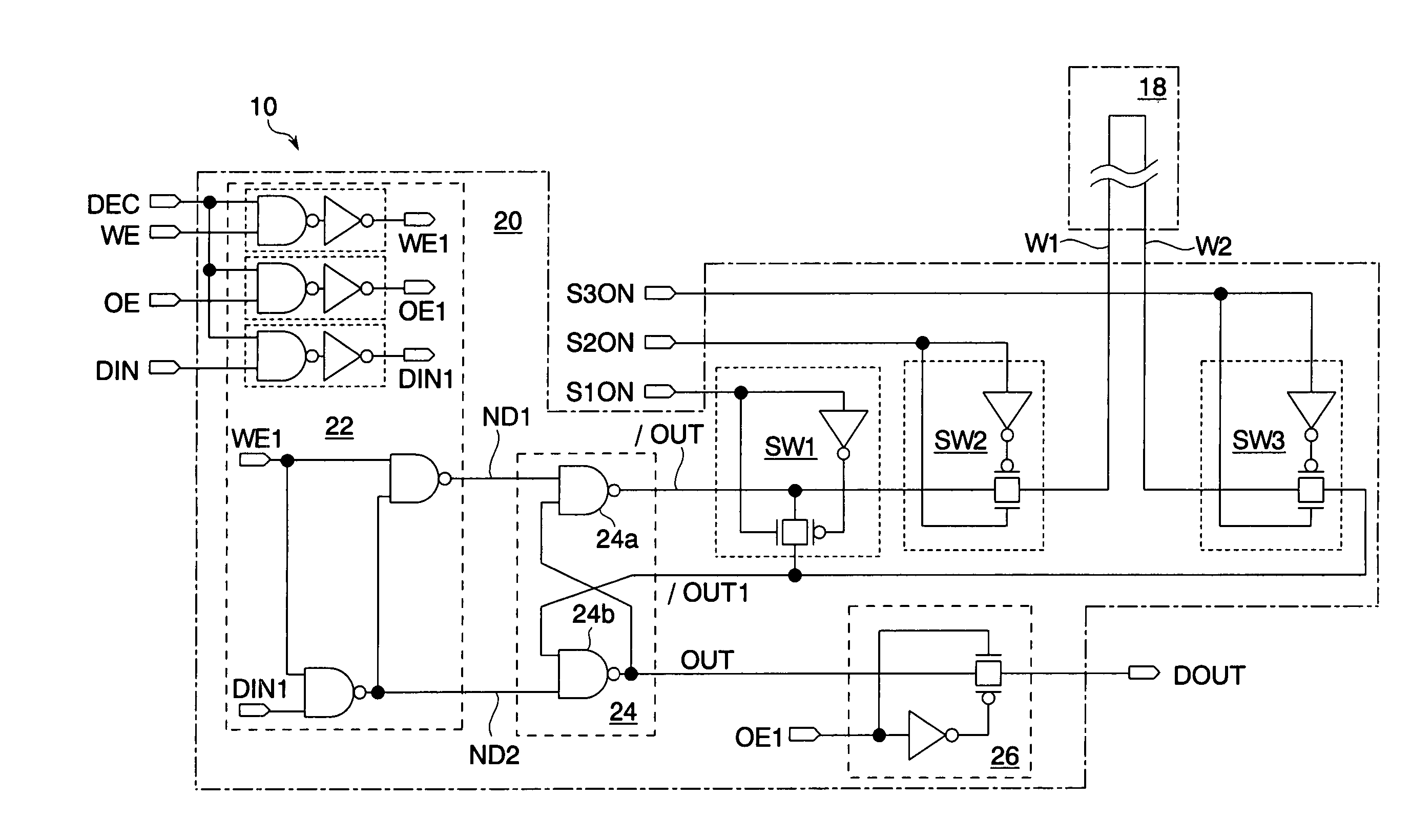
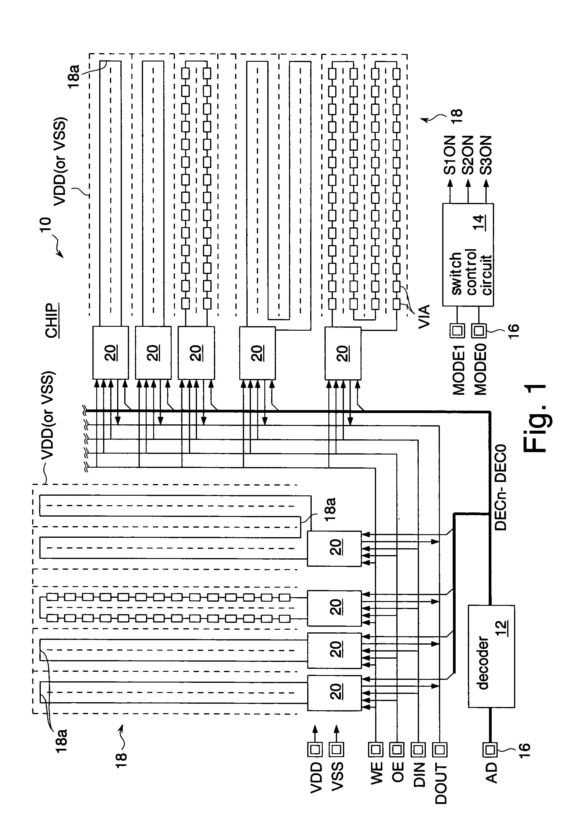
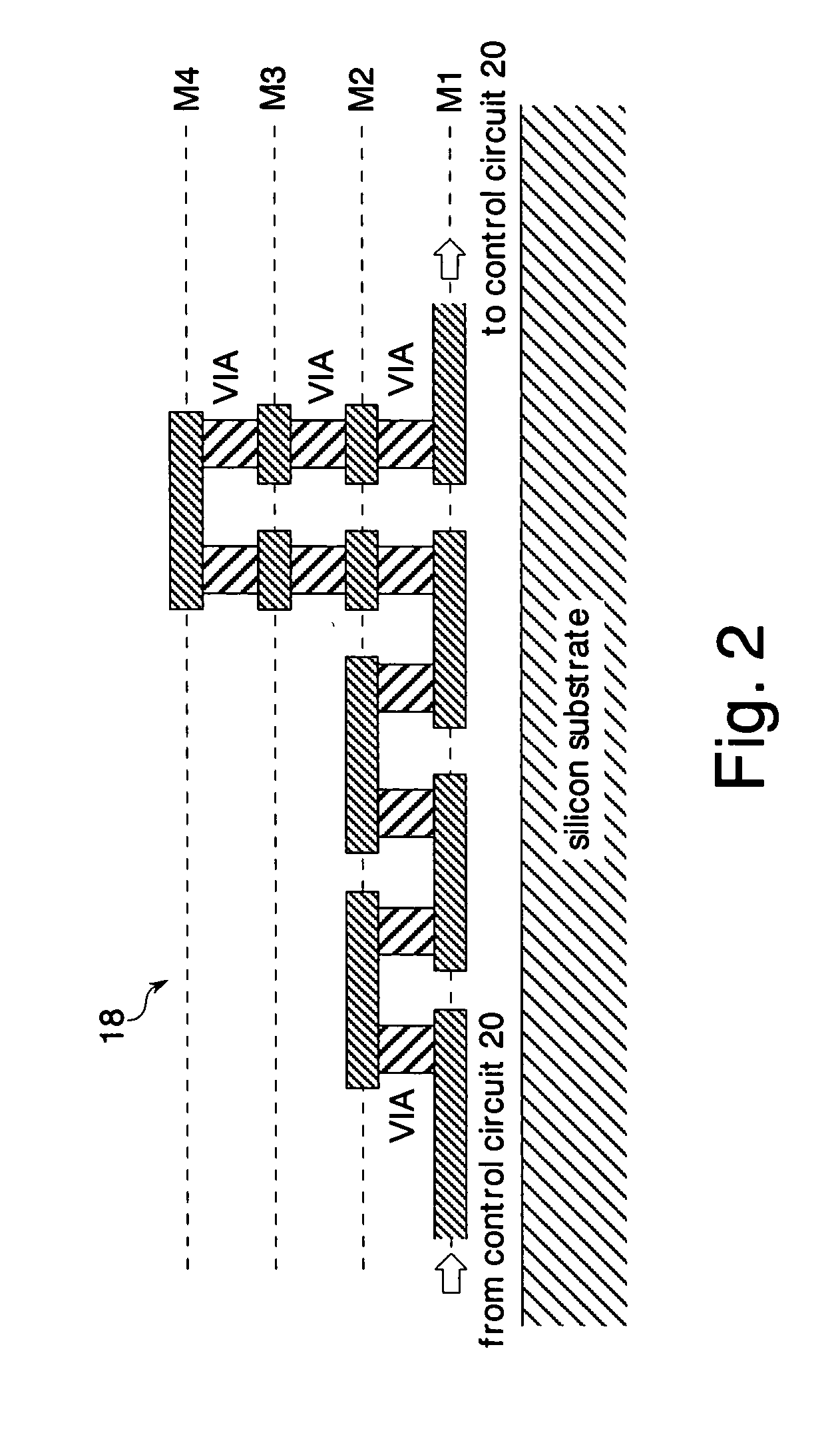
[0037]FIG. 1 shows the semiconductor integrated circuit of the present invention. This semiconductor integrated circuit is formed on a silicon substrate as an evaluation chip CHIP for evaluating a semiconductor fabrication process, through the use of a CMOS process. On the evaluation chip CHIP, provided are wiring evaluation circuits 10 for evaluating the shape of wiring formed on the chip, an element evaluation circuit (not shown) for evaluating the characteristics of elements such as transistors and resistors, and so on. The element evaluation circuit evaluates an electrical characteristic (DC characteristic) of a single element and a performance characteristic (AC characteristic) of a circuit constituted of a plurality of elements. Each of the wiring evaluation circuits 10 evaluates a process condition under which a break occurs in the wiring and a process condition under which a short occurs in the wiring. In other words, the process conditions and process margins are evaluated ...

second embodiment

[0087]This embodiment is different from the second embodiment in a logic signal supplied to the other end W2 of an evaluation wiring 18 via a switch circuit SW4 of the control circuit 20B. Specifically, an input of the switch circuit SW4 is connected to a node IN1 instead of a node / OUT.

[0088]The node IN1 is directly connected to, for example, an external terminal. A voltage of the node IN1 is directly set by an LSI tester connected to an evaluation chip. The other configuration is the same as that of the second embodiment. The formation of the node IN1 connected to the external terminal makes it possible to give a desired voltage to the node IN1 in a write operation of a break / short mode. As a result, more detailed evaluation can be executed in the break / short mode.

[0089]In this embodiment, the same effects as those in the above-described first and second embodiments are also obtainable.

[0090]FIG. 11 shows a fourth embodiment of the semiconductor integrated circuit of the present i...


PUM


Abstract

An input circuit writes an expected value to one end of an evaluation wiring. A latch circuit latches a logic level of the other end of the evaluation wiring. A first switch circuit connects an output of the input circuit to the input of the latch circuit. A second switch circuit connects the output of the input circuit to the one end of the evaluation wiring. A third switch circuit connects the other end of the evaluation wiring to the input of the latch circuit. By turning on, off, and off the first to third switch circuits, respectively, the output of the input circuit is directly connected to only the input of the latch circuit. In this state, the input circuit writes an expected value, and a logic level is read from the latch circuit. Accordingly, failure of the evaluation wiring can be easily discriminated from other failure.

Description

CROSS-REFERENCE TO RELATED APPLICATIONS[0001]This application is based upon and claims the benefit of priority from the prior Japanese Patent Application No. 2003-427603, filed on Dec. 24, 2003, the entire contents of which are incorporated herein by reference.BACKGROUND OF THE INVENTION[0002]1. Field of the Invention[0003]The present invention relates to a semiconductor integrated circuit having a wiring evaluation circuit for evaluating wiring formed on a chip when a semiconductor fabrication process or the like is developed, and to an evaluation method of the wiring in the semiconductor integrated circuit.[0004]2. Description of the Related Art[0005]When a new semiconductor fabrication process is developed, an evaluation chip is generally used to evaluate the shape of wiring fabricated by this process, the characteristics of elements, and so on. On the evaluation chip, a wiring evaluation circuit, an element evaluation circuit, and so on are formed. In the wiring evaluation circu...

Claims


Application Information

Patent Timeline
Patent Type & Authority Patents(United States)
IPC IPC(8): G01R31/08G06F11/00G01R31/28H01L21/66H01L21/822H01L23/544H01L27/04
CPCH01L22/34G01R31/2853H01L2924/0002H01L2924/00
Inventor IGETA, MITSUAKIWAKAYAMA, SHIGETOSHIENDOU, SEIJI
Owner FUJITSU LTD
Why Eureka
Try Eureka