Method of fabricating semiconductor integrated circuit device and method of producing a multi-chip module that includes patterning with a photomask that uses metal for blocking exposure light and a photomask that uses organic resin for blocking exposure light

multi-chip technology, applied in the field of manufacturing a semiconductor integrated circuit device and a multi-chip module, can solve the problems of affecting the improvement of the productivity of the semiconductor integrated circuit device, affecting the reduction of the fabrication cost, and requiring a large amount of time and increased costs to fabricate the mask, etc., to achieve good durability, and reduce the cost of manufacturing. cost

Inactive Publication Date: 2005-02-01
RENESAS ELECTRONICS CORP
View PDF5 Cites 2 Cited by
  • Summary
  • Abstract
  • Description
  • Claims
  • Application Information

AI Technical Summary

Benefits of technology

Specifically, the mask having an opaque pattern made of a metal film is advantageous in mass production because it has good durability and high reliability and is capable of being used in a large amount of exposure. However, when such a mask is used in the development period of a semiconductor integrated circuit device or in the fabrication of a small number of various semiconductor integrated circuit devices, in other words, in the case where changes and modifications are frequently made in the mask pattern and the same mask is rarely used in different processes, a great amount of time and increased cost are required to fabricate the mask. Therefore, there arise such problems as to hinder the improvement in productivit

Problems solved by technology

However, when such a mask is used in the development period of a semiconductor integrated circuit device or in the fabrication of a small number of various semiconductor integrated circuit devices, in other words, in the case where changes and modifications are frequently made in the mask pattern an

Method used


Image

  • Method of fabricating semiconductor integrated circuit device and method of producing a multi-chip module that includes patterning with a photomask that uses metal for blocking exposure light and a photomask that uses organic resin for blocking exposure light
  • Method of fabricating semiconductor integrated circuit device and method of producing a multi-chip module that includes patterning with a photomask that uses metal for blocking exposure light and a photomask that uses organic resin for blocking exposure light
  • Method of fabricating semiconductor integrated circuit device and method of producing a multi-chip module that includes patterning with a photomask that uses metal for blocking exposure light and a photomask that uses organic resin for blocking exposure light

Examples


first embodiment

(First Embodiment)

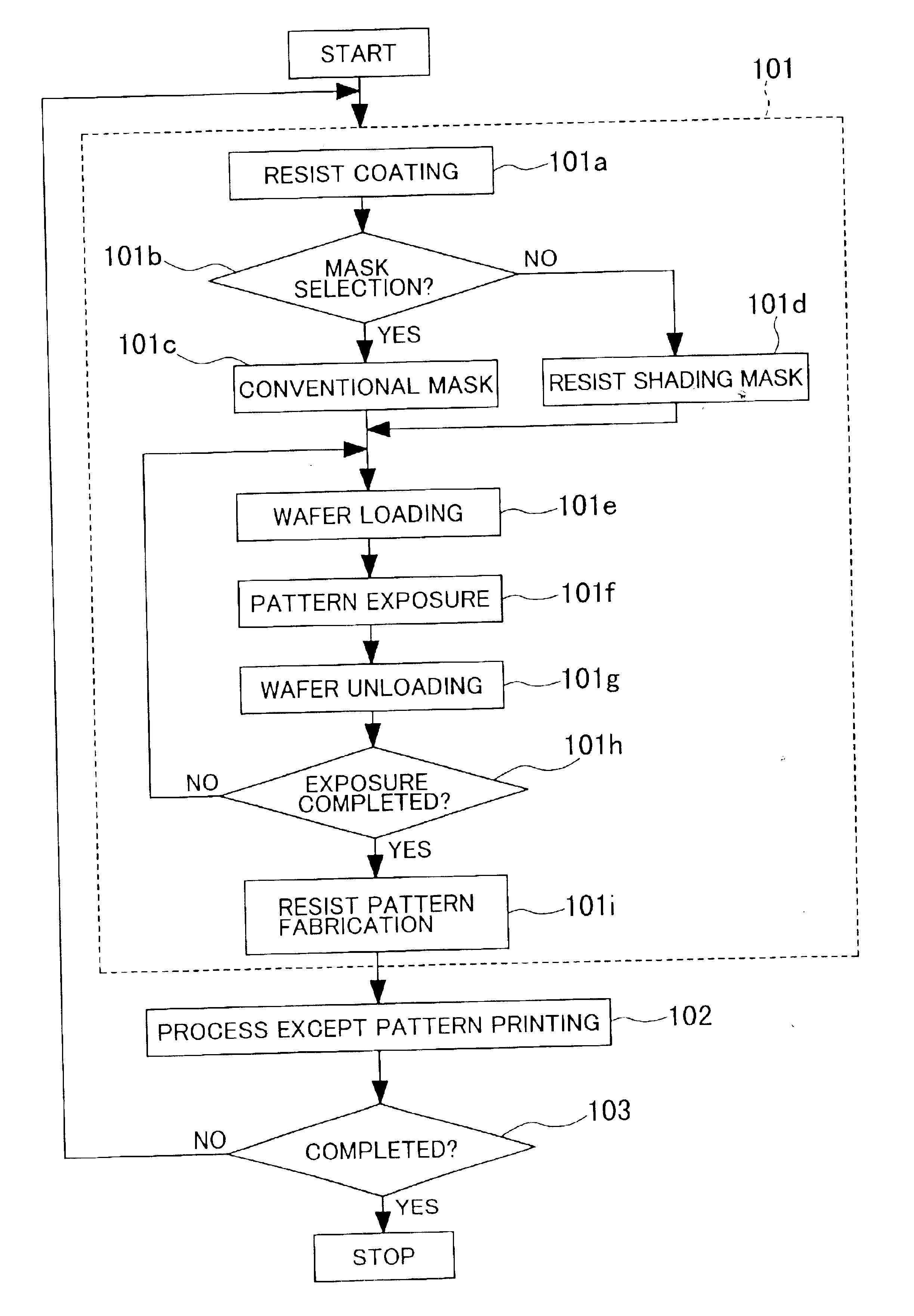
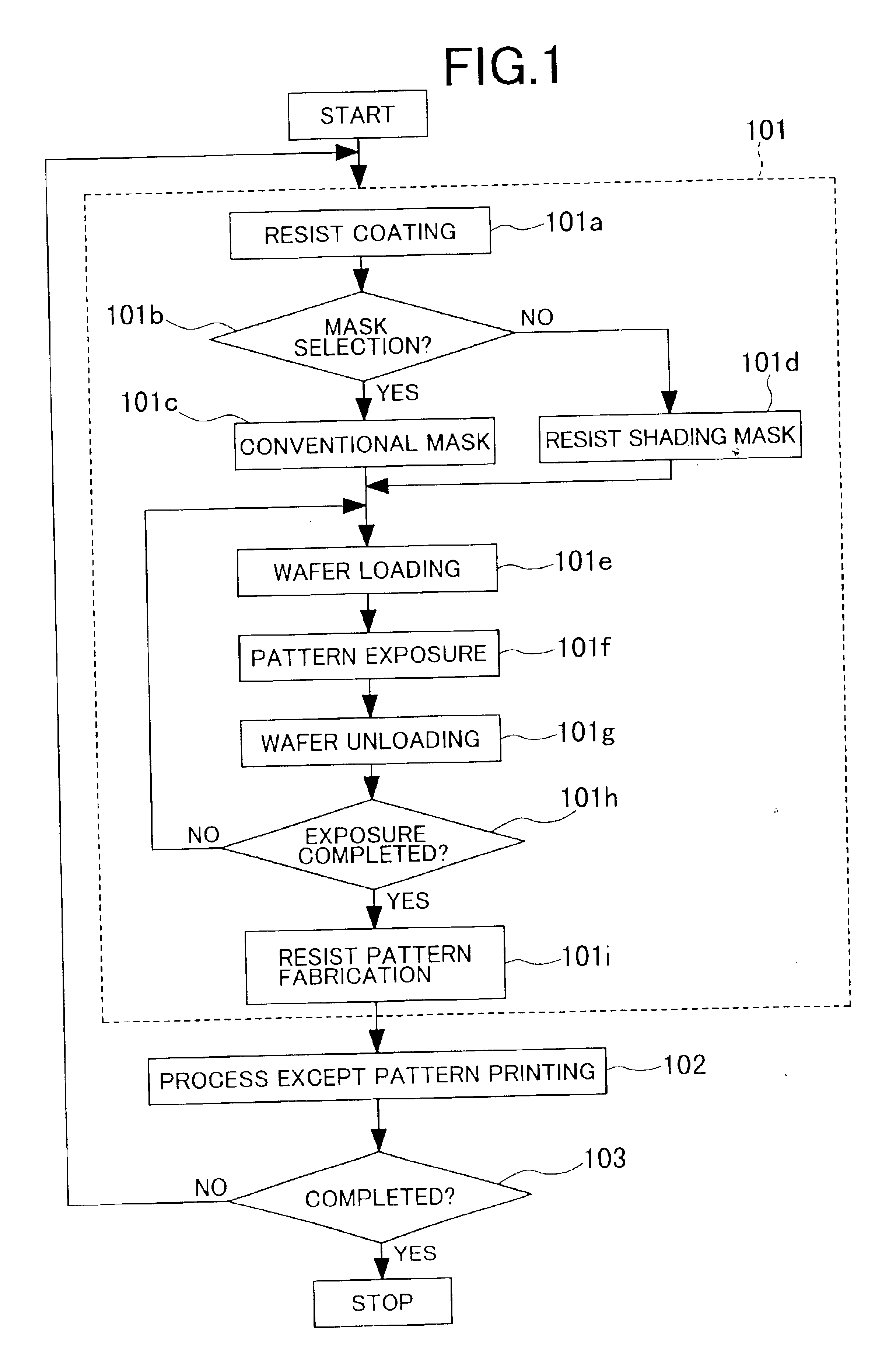
First, a method of fabricating a semiconductor integrated circuit device according to an embodiment of the present invention will be described by the use of FIG. 1. Step 101 is a pattern printing step in which a pattern formed on a mask is printed onto a wafer, and step 102 is a step in which various processes such as etching, impurity doping, deposition, and the like are performed. In the conventional semiconductor integrated circuit device, the pattern printing (exposure) and the various processes are repeatedly performed until it is determined that all of the steps are completed in step 103.

Now, in this embodiment, in the pattern printing step 101, after coating of a resist film on a main surface of a wafer (step 101a), which one of the above-mentioned conventional mask (first photomask) and the above-mentioned resist shading mask (second photomask) is used is selected (step 101b). In this case, for example, when the number of wafers to be exposed (the number of...

second embodiment

(Second Embodiment)

In this embodiment, descriptions will be made of the case where the technical idea of the present invention is applied to the fabrication of, for example, a mask ROM.

The mask ROM has characteristics as follows. That is, a large capacity memory can be achieved because a memory cell is formed of one MIS, and the entire circuit structure thereof can be made simple because no writing operation is required. However, since the contents of memory differ in accordance with the demands of customers, TAT of the mask ROM becomes longer in comparison to that of another ROM (e.g., EEPROM (Electric Erasable Programmable Read Only Memory)) and different masks must be fabricated for respective various kinds of ROM codes of the customers. Therefore, there arises such a problem that the product cost is increased in the small-lot production. Thereupon, in this embodiment, patterns of base data constituted by basic components common to various kinds of mask ROMs are printed by the us...

third embodiment

(Third Embodiment)

This embodiment is a modification example of the second embodiment, and will describe the case where the present invention is applied to the fabrication method of the mask ROM of data rewriting type, which is different from that of the second embodiment.

FIGS. 67A to 67C show base data of a mask ROM used in this embodiment. FIG. 67A is a plan view showing the layout of the memory cell region, FIG. 67B is a circuit diagram of the same, and FIG. 67C is a cross-sectional view taken along line A—A in FIG. 67A. In this embodiment, a mask ROM of the contact hole programming type is exemplified. In this mask ROM of the contact hole programming type, programming is performed according to how to lay out contact holes (represented by the dashed line in FIG. 67B) which connect the respective semiconductor regions 11n and the data line DL. Also in this embodiment, the conventional mask is used to print the pattern of the base data.

The contact holes for rewriting described below...


PUM


Abstract

Productivity of a semiconductor integrated circuit device is improved. According to how many times the photomask is used, a photomask having an opaque pattern made of metal and a photomask having an opaque pattern made of a resist film are properly used, and thereby an exposure treatment is performed.

Description

BACKGROUND OF THE INVENTIONThe present invention relates to a method of fabricating a semiconductor integrated circuit device and a method of fabricating a multichip module, more particularly, to a technique effectively applicable to a photolithography (hereinafter, referred to as lithography) technique in which a predetermined pattern is printed onto a semiconductor wafer (hereinafter, referred to as wafer) with using a photomask (hereinafter, referred to as mask) in the fabrication process of a semiconductor integrated circuit device.In the fabrication of a semiconductor integrated circuit device (LSI: Large Scale Integrated Circuit), the lithography technique is used as a method of forming a fine pattern on a wafer. As the lithography technique, a so-called optical projection exposure method, in which a pattern formed on each mask is repeatedly printed onto a wafer through reduced projection optics, has become the mainstream. The basic constitution of the exposure tool is disclos...

Claims


Application Information

Patent Timeline
IPC IPC(8): G03F1/10G03F1/08G03F1/14G03F1/54G03F1/56G03F7/20H01L21/768
CPCG03F1/14G03F1/56G03F7/70425Y10S438/946Y10S438/944G03F1/00H01L24/05H01L2224/05001H01L2224/05008H01L2224/05022H01L2224/05024H01L2224/05569H01L2224/05572H01L2224/06131H01L2224/16225H01L2224/32225H01L2224/73204H01L2224/92125H01L2924/15311H01L2924/00H01L21/027
Inventor TERASAWA, TSUNEOTANAKA, TOSHIHIKOMIYAZAKI, KOHASEGAWA, NORIOMORI, KAZUTAKA
Owner RENESAS ELECTRONICS CORP
Why Eureka
Try Eureka