

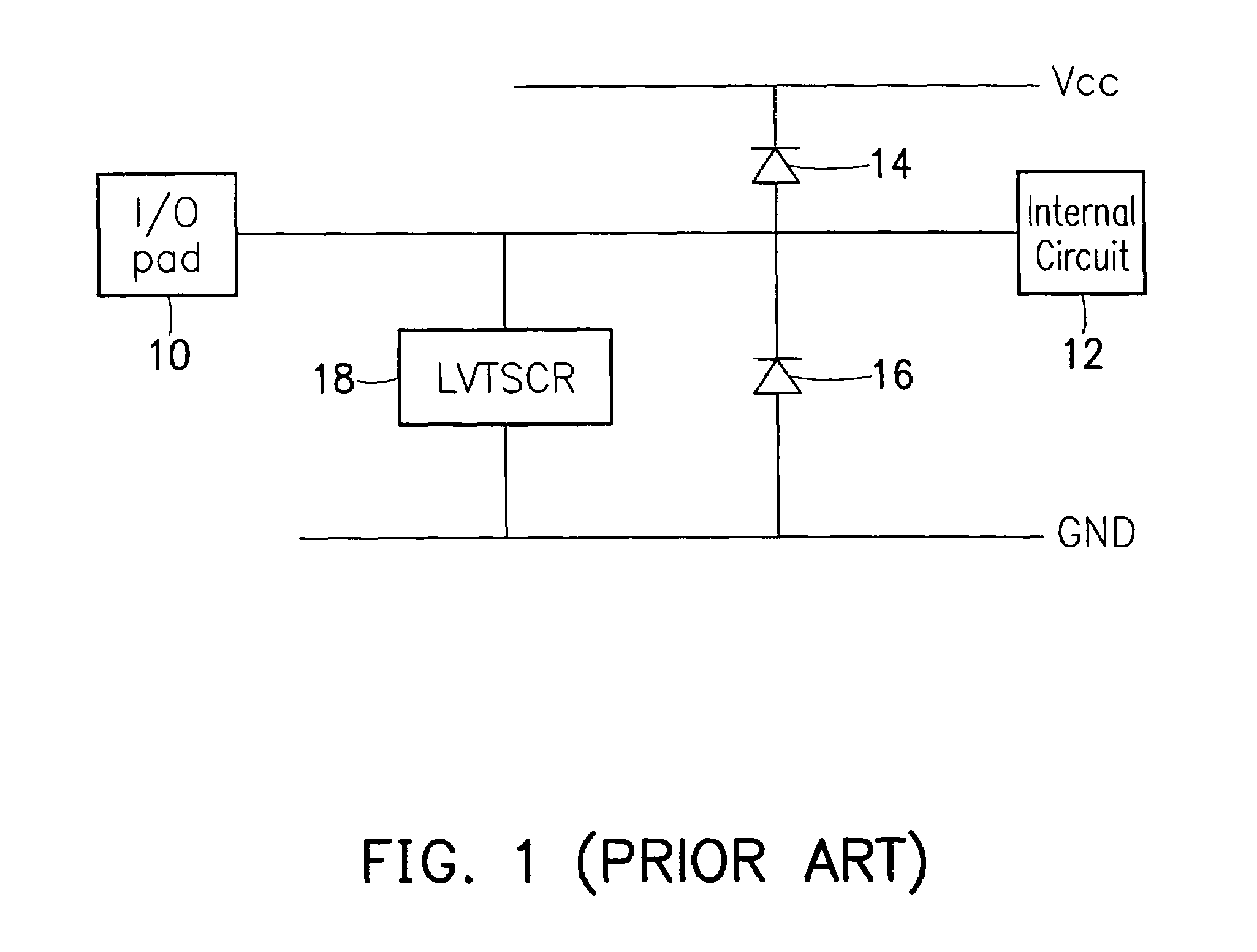
Electrostatic discharge protection circuit coupled on I/O pad
a protection circuit and electrostatic discharge technology, applied in the direction of emergency protective arrangements for limiting excess voltage/current, emergency protective arrangements, and arrangements responsive to excess voltage, can solve the problems of esd protection circuit to be temporarily or permanently unable to work, and the failure of esd protection circuit, so as to achieve effective avoidance of the catch-up phenomenon
- Summary
- Abstract
- Description
- Claims
- Application Information
AI Technical Summary
Benefits of technology
Problems solved by technology
Method used
Image

Examples
example 1
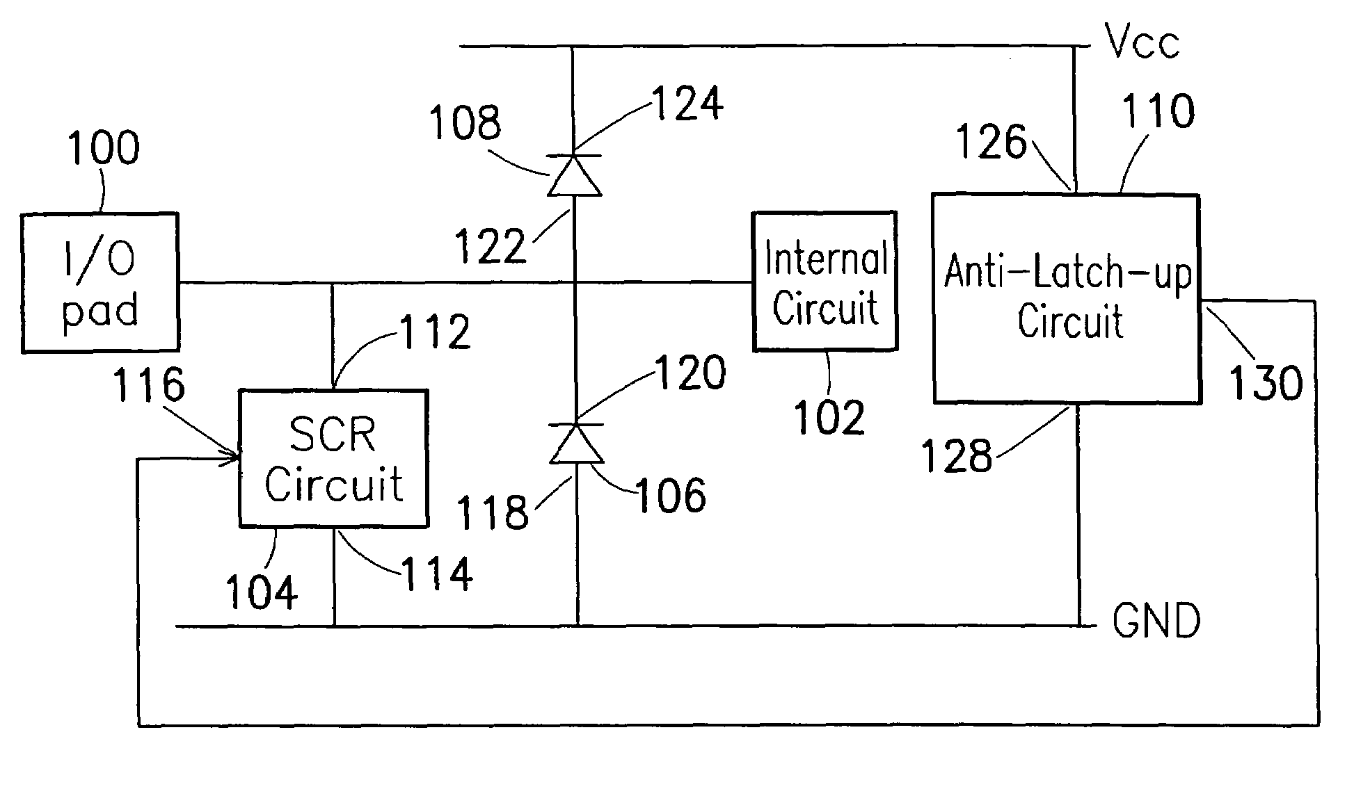
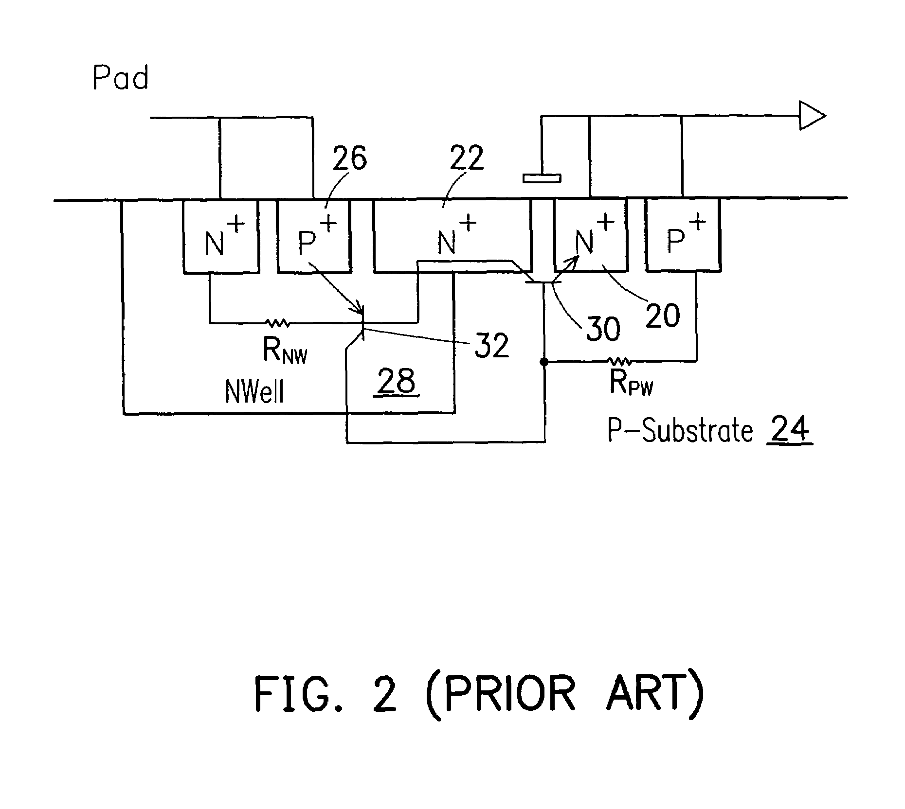
[0044]FIGS. 5A–5B are circuit diagrams, schematically the semiconductor structures of the I / O pad ESD protection circuit, according to a first preferred embodiment of the invention. In FIG. 4 as described previously, a relationship between the SCR circuit 104 and the anti-latch circuit 110 has been described, where the diode effect is not well described. In FIG. 5A, the SCR circuit in a semiconductor structure includes a p-type substrate 150, an N well 152, a first P+ doped region 154, a first N+ doped region 156, a second N+ doped region 158, a second P+ doped region 160, and a third N+ doped region 162, where the p-type substrate 150 can also represents a P well.
[0045]The N well 152 is formed in the p-type substrate 150. The first P+ doped region 154 is formed in the p-type substrate 150, and is coupled to the ground voltage. The first N+ doped region 156 is formed in the p-type substrate 150 adjacent to the first P+ doped region 154, and is coupled to the ground voltage. The firs...
example 2
[0050]FIGS. 6A–6B are circuit diagrams, schematically the semiconductor structures of the I / O pad ESD protection circuit, according to a second preferred embodiment of the invention. In this Example 2, the SCR circuit remain the same. In the following, the same numeral reference represent the similar element. The description about SCR circuit is skipped here. The difference of the anti-latch-up circuit 200 from the Example 1 is the additional PMOS transistor 202 that has a source region coupled to the voltage source Vcc, a drain region coupled to the second N+ doped region 158, and a resistor 204 with a first end 206 and a second end 208, respectively coupled to a gate electrode of the PMOS transistor 202 and the ground voltage. In addition, a capacitor 210 has a first contact end 212 and a second contact end 214, respectively coupled to the voltage source Vcc and the gate of the PMOS transistor 202.
[0051]Similarly to the Example 1, the RC delay time of the anti-latch-up circuit is ...
example 3
[0053]FIGS. 7A–7B are circuit diagrams, schematically the semiconductor structures of the I / O pad ESD protection circuit, according to a third preferred embodiment of the invention. In this Example 3, the SCR circuit is modified into a LVTSCR circuit. Comparison with the SCR circuit in Example 2 as shown in FIGS. 6A–6B, the LVTSCR circuit includes an additional NMOS transistor 256.
[0054]The LVTSCR circuit includes in a semiconductor structure includes a p-type substrate 150, an N well 152, a first P+ doped region 154, a first N+ doped region 156, a second N+ doped region 158, a second P+ doped region 160, and a third N+ doped region 162, where the p-type substrate 150 can also represents a P well.
[0055]The N well 152 is formed in the p-type substrate 150. The first P+ doped region 154 is formed in the p-type substrate 150, and is coupled to the ground voltage. The first N+ doped region 156 is formed in the p-type substrate 150 adjacent to the first P+ doped region 154, and is couple...
PUM
 Abstract
Description
Claims
Application Information