Metal gate transistor CMOS process and method for making

a metal gate transistor and metal gate technology, applied in the direction of transistors, semiconductor devices, electrical equipment, etc., can solve the problems of metal oxide loss oxygen, change of change of the vsub>t /sub> of the devi

Inactive Publication Date: 2006-09-19
NORTH STAR INNOVATIONS
View PDF6 Cites 70 Cited by
  • Summary
  • Abstract
  • Description
  • Claims
  • Application Information

AI Technical Summary

Problems solved by technology

One problem with the use of a conductive metal oxide as a gate material is that the metal oxide may lose oxygen during high temperature annealing, i.e. over 450 degrees Celsius.
The undesirable loss of oxygen causes the work function of the gate to change, thus changing the VT of the device.

Method used


Image

  • Metal gate transistor CMOS process and method for making
  • Metal gate transistor CMOS process and method for making
  • Metal gate transistor CMOS process and method for making

Examples


Embodiment Construction

[0018]Generally, the present invention overcomes the previously described problem of the gate electrode losing oxygen during high temperature annealing by including an oxidation resistant barrier layer over the conductive gate oxide. A polysilicon capping layer is deposited over the oxidation resistant barrier layer so that the gate salicide process can be formed in a conventional manner.

[0019]These benefits and advantages will be more readily understood upon reading of the following detailed description when taken in conjunction with the respective illustrations. It is noted that the illustrations are not drawn to scale in all respects but accuracy in scale is not necessary for understanding the invention. Furthermore, there are likely to be other embodiments within the scope of the invention that are not specifically illustrated.

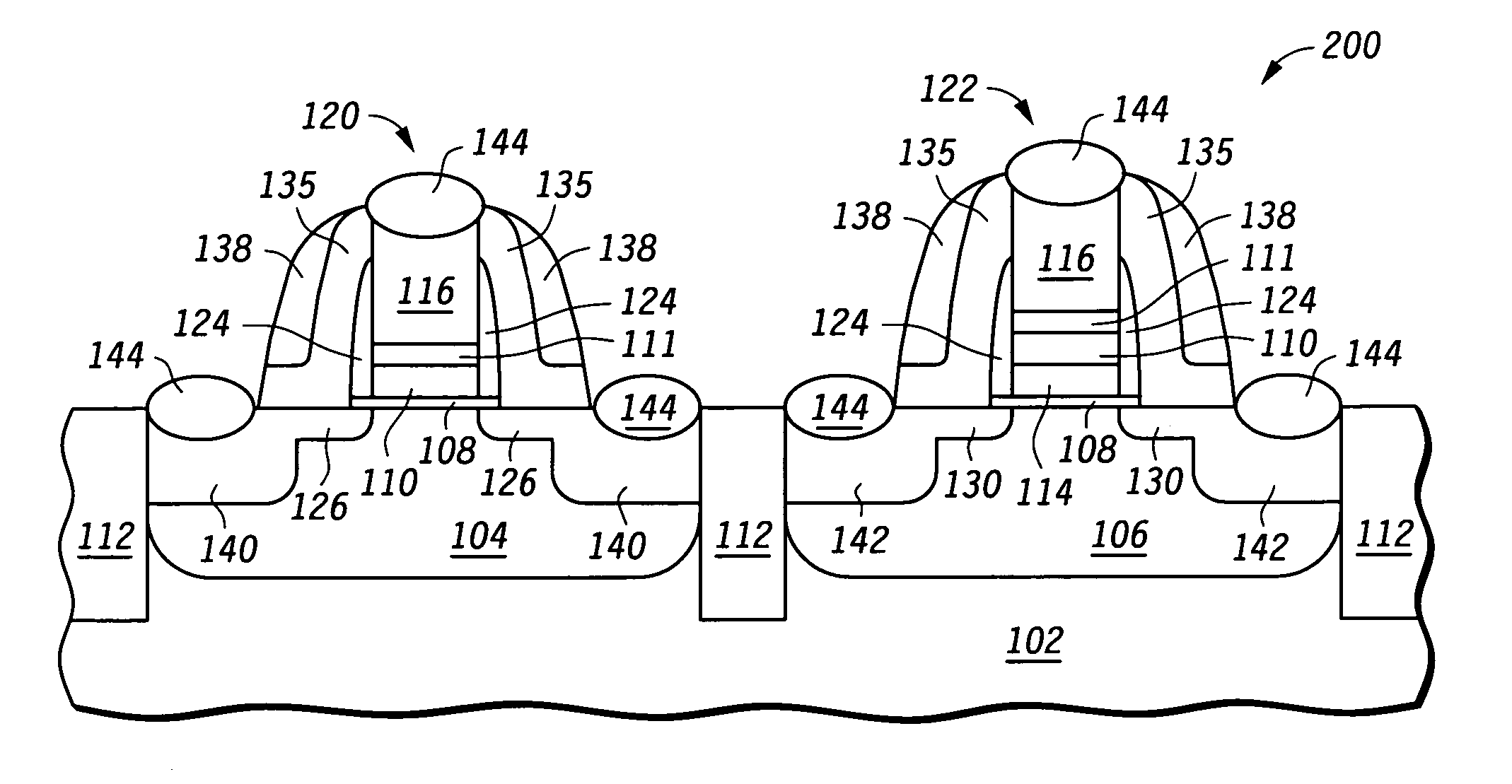
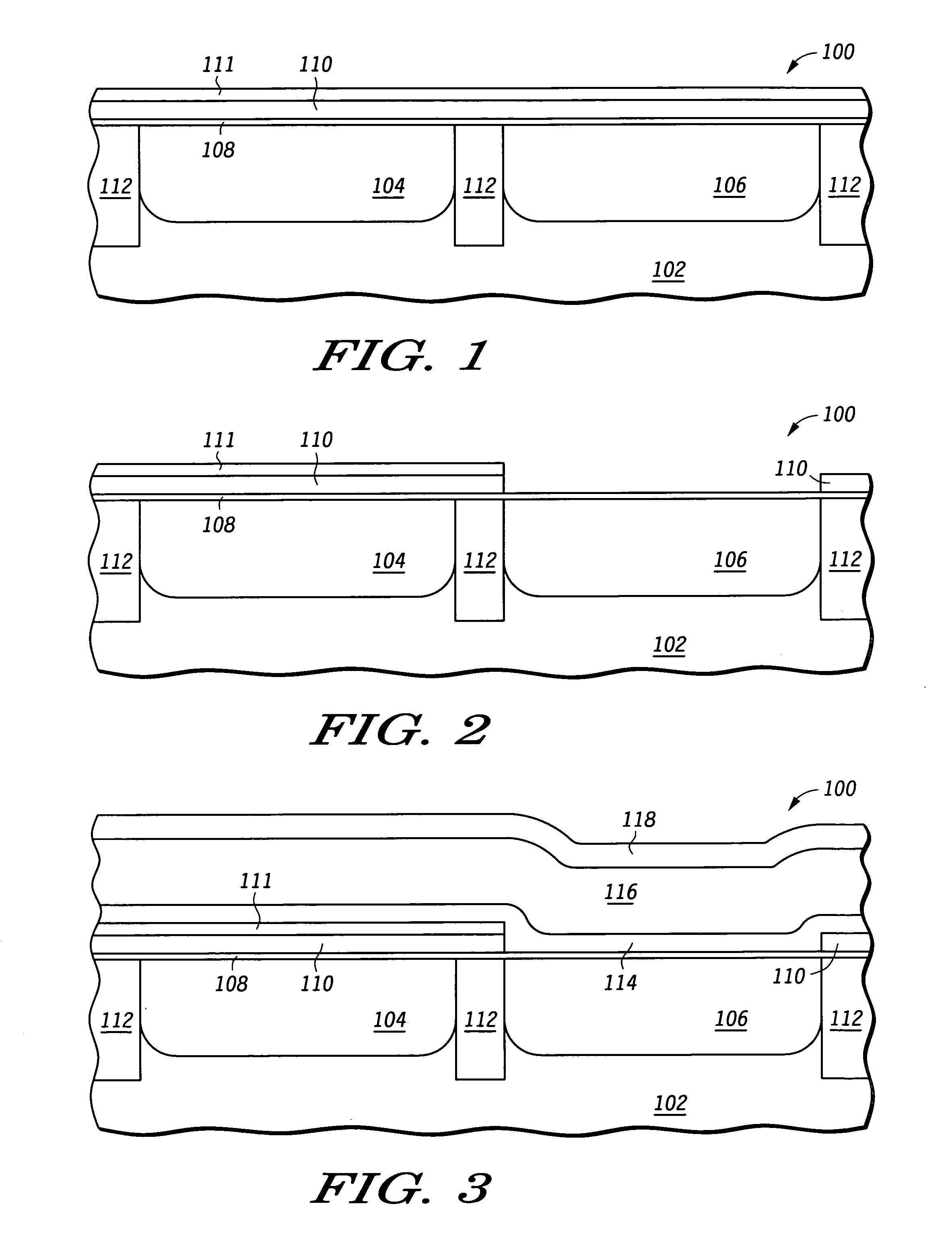
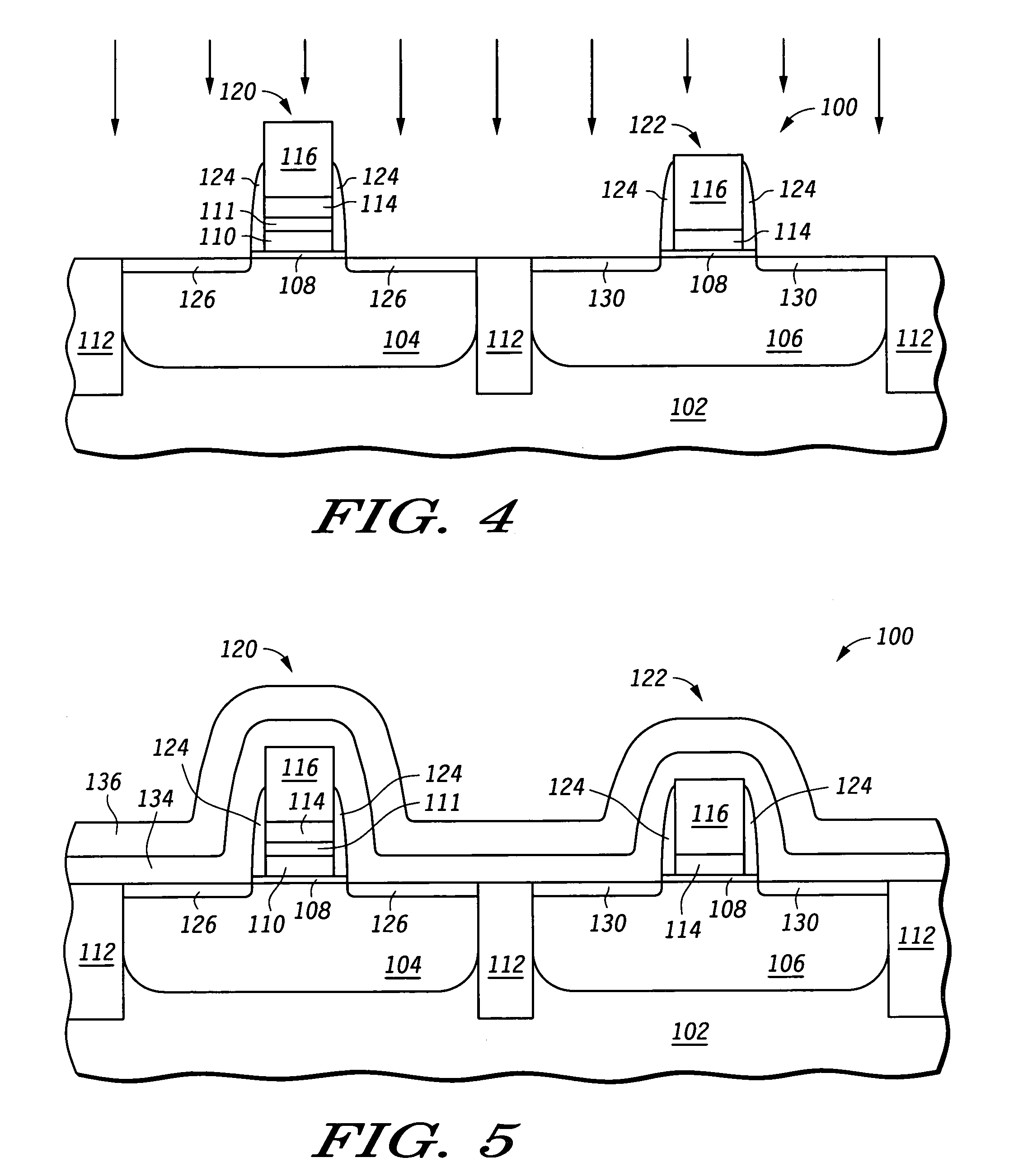
[0020]FIGS. 1–7 illustrate cross sectional views at various stages of one embodiment of a semiconductor process according to the present invention. In FIG...


PUM

PropertyMeasurementUnit
temperatureaaaaaaaaaa
thicknessaaaaaaaaaa
work functionaaaaaaaaaa

Abstract

A method for forming a semiconductor device (100) includes a semiconductor substrate (102) having a first region (104), forming a gate dielectric (108) over the first region, forming a conductive metal oxide (110) over the gate dielectric, forming an oxidation resistant barrier layer (111) over the conductive metal oxide, and forming a capping layer over the oxidation resistant barrier layer. In one embodiment, the conductive metal oxide is IrO2, MoO2, and RuO2, and the oxidation resistant barrier layer includes TiN.

Description

CROSS-REFERENCE TO RELATED APPLICATION[0001]The present application is related to a commonly assigned, co-pending application by Taylor et al. entitled, “Blocking Layer For Silicide Uniformity in a Semiconductor Transistor”, and filed Dec. 18, 2003 as U.S. Ser. No. 10 / 739,684.[0002]1. Field of the Invention[0003]The present invention is related to the field of semiconductor fabrication and more particularly to gate metals for NMOS (n-channel metal oxide semiconductor) and PMOS (p-channel MOS) devices.[0004]2. Related Art[0005]In the field of CMOS (complementary metal-oxide semiconductor) fabrication, the use of gates containing both a metal and an oxide is being considered. In a dual metal gate process, a first metal is used to form the gate electrodes for PMOS devices while a second different metal is used to form the gate electrodes for NMOS devices. The reason for using differing metals is so that the work functions can be optimized for each type of device. Changes in work functi...

Claims


Application Information

Patent Timeline
Patent Type & Authority Patents(United States)
IPC IPC(8): H01L21/8238H01L29/76
CPCH01L21/823835H01L21/823864H01L21/823842H01L27/092
Inventor SCHAEFFER, III, JAMES K.ADETUTU, OLUBUNMI O.
Owner NORTH STAR INNOVATIONS
Why Eureka
Try Eureka