Crackstop with release layer for crack control in semiconductors

a technology of crack stop and release layer, which is applied in the direction of liquid surface applicators, semiconductor/solid-state device details, coatings, etc., can solve the problems of cracks that damage the active area of chips, insulator material mechanically weakening, and it is significantly easier for crack stop/edge seal to be breached

Inactive Publication Date: 2006-09-19
GLOBALFOUNDRIES INC
View PDF6 Cites 33 Cited by
  • Summary
  • Abstract
  • Description
  • Claims
  • Application Information

AI Technical Summary

Benefits of technology

[0006]Another object of the present invention is to provide methods of forming and at least one vertical interface that deflects cracks generated during integrated circuit fabrication, and in particular during dicing, and thereby preventing any cracks from penetrating into a crack stop.
[0008]It is yet another object of the present invention to provide methods of forming integrated circuits having at least one vertical interface that reduces the real estate required for crack stops by making crack stops more effective, thereby enabling fewer crack stops to be used such that a greater number of chips can be produced per wafer.
[0009]It is another object of the present invention to provide strong, reliable and efficient semiconductor chips having at least one vertical interface in close proximity to a crack stop.
[0011]The above and other objects, which will be apparent to those skilled in art, are achieved in the present invention, which is directed to in a first aspect, a method of controlling cracks in a semiconductor device. The method at least includes providing an integrated circuit structure having a crack stop along its perimeter. At least one opening is formed adjacent to the crack stop, and a release material is deposited in an amount sufficient to at least fill the opening. Excess release material is then removed to form a vertical interface within the opening adjacent to the crack stop, which acts to prevent cracks from penetrating into the crack stop.
[0012]The release material may be a material having low adhesion strength to adjoining layers enabling such cracks to be deflected away from the crack stop, whereby penetration of the crack into the crack stop is avoided. Alternatively, the release material may be a material having a sufficient toughness to enable the vertical interface to control the cracks in the semiconductor by absorbing the cracks, thereby preventing the cracks from penetrating the crack stop.
[0017]In another aspect, the invention is directed to another method of controlling cracks in an integrated circuit device by providing a wiring level having an ultra low-k dielectric layer and a crack stop within the ultra low-k dielectric layer along the perimeter. The ultra low-k dielectric layer within a vertical channel adjacent the crack stop is located and then modified to form a self-aligned vertical interface. This self-aligned vertical interface controls cracks by preventing the cracks from penetrating into the crack stop. The ultra low-k dielectric layer may be modified by either collapsing such dielectric layer to form a void adjacent the crack stop thereby weaken adhesion of the ultra low-k dielectric layer to the crack stop, or it may be modified by increasing toughness of the ultra low-k dielectric for absorbing any crack energies.

Problems solved by technology

The dicing process often causes cracks that damage active areas of the chips.
However, as the dielectric constant of the material is lowered, the insulator material becomes mechanically weaker, and as such, it becomes significantly easier for the crack stop / edge seal to be breached.
However, this type of conventional approach takes up valuable “real estate” on the chip, ultimately reducing the number of chips that can be produced per wafer.

Method used


Image

  • Crackstop with release layer for crack control in semiconductors
  • Crackstop with release layer for crack control in semiconductors
  • Crackstop with release layer for crack control in semiconductors

Examples


Embodiment Construction

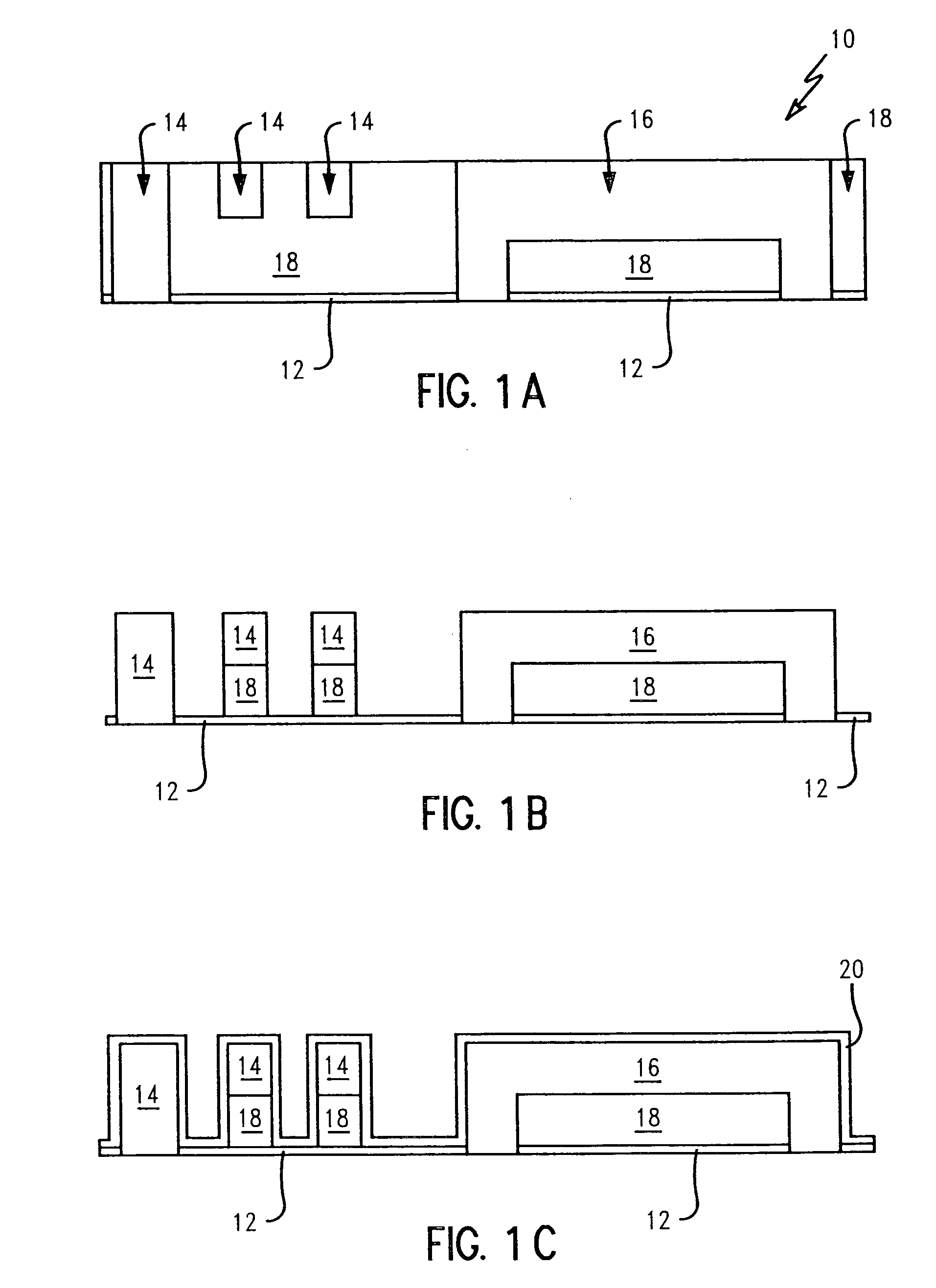
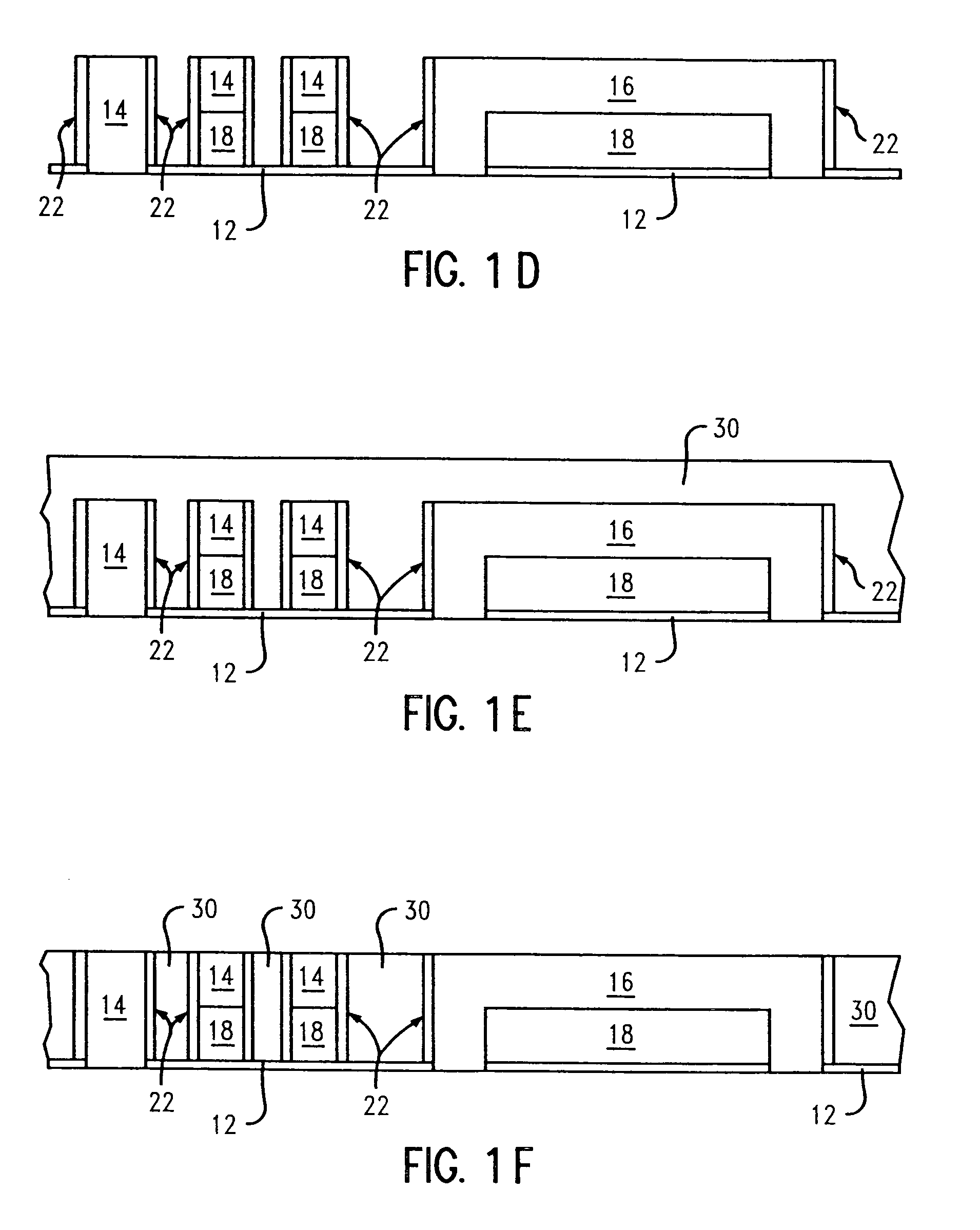
[0027]In describing the preferred embodiment of the present invention, reference will be made herein to FIGS. 1A–5C of the drawings in which like numerals refer to like features of the invention.

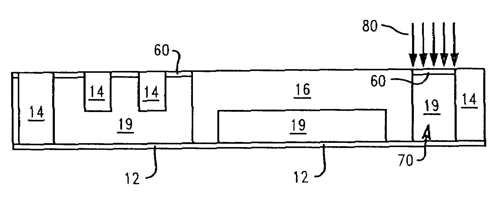
[0028]Crack stops are often incorporated around the perimeter of chips for preventing damage or cracks from reaching the active areas of the chips during dicing. The present invention provides a vertical interface adjacent to an existing crack stop around a perimeter of a chip, such as a metal crack stop having a pyramid design. The vertical interface of the invention controls cracks emanating from diced edges from traversing through, i.e., cracking, the crack stop, as well as controls cracks as a result of packaged-induced stresses in service.

[0029]The vertical interface is comprised of a material that prevents generated cracks from damaging the crack stop by deflecting any generated cracks from entering into the crack stop or by absorbing the generated cracks. The vertical interface also m...


PUM


Abstract

Methods of forming and the integrated circuit device structure formed having vertical interfaces adjacent an existing crack stop around a perimeter of a chip, whereby the vertical interface controls cracks generated during side processing of the device such as dicing, and in service from penetrating the crack stop. The vertical interface is comprised of a material that prevents cracks from damaging the crack stop by deflecting cracks away from penetrating the crack stop, or by absorbing the generated crack energies. Alternatively, the vertical interface may be a material that allows advancing cracks to lose enough energy such that they become incapable of penetrating the crack stop. The present vertical interfaces can be implemented in a number of ways such as, vertical spacers of release material, vertical trenches of release material or vertical channels of the release material.

Description

BACKGROUND OF INVENTION[0001]The present invention relates to semiconductor substrates, and more particularly, to methods and semiconductor structures having a release layer for controlling cracks that form during dicing or as a result of package-induced stresses.[0002]Integrated circuits are fabricated by building multiple layers of wiring and passivation on substrates (wafers) that contain semiconductor devices. Upon completion of substrate-level processing, wafers are diced to provide individual chips. The dicing process often causes cracks that damage active areas of the chips. To prevent such damage, crack stop layers have been employed along the perimeter of the chip.[0003]These crack stop layers often take on additional functions for low-K dielectrics, such as providing an edge seal to prevent moisture ingress that can damage or destroy active areas of a chip. They also protect active areas of chips from cracks, which may emanate from the diced edges as a result of package-in...

Claims


Application Information

Patent Timeline
Patent Type & Authority Patents(United States)
IPC IPC(8): H01L21/76H01L21/82B05D1/02H01L21/78H01L23/00
CPCH01L21/78H01L23/562H01L2924/0002H01L2924/00
Inventor FITZSIMMONS, JOHN A.LANE, MICHAEL W.MCGAHAY, VINCENT J.SHAW, THOMAS M.STAMPER, ANTHONY K.
Owner GLOBALFOUNDRIES INC
Why Eureka
Try Eureka