Method for inspecting substrate, substrate inspecting system and electron beam apparatus

a substrate inspection and electron beam technology, applied in material analysis using wave/particle radiation, instruments, nuclear engineering, etc., can solve the problems of high inspection speed, low inspection speed, and low throughput of electron beam inspection apparatus, and achieve high throughput and high reliability

Inactive Publication Date: 2006-09-19
EBARA CORP
View PDF29 Cites 155 Cited by
  • Summary
  • Abstract
  • Description
  • Claims
  • Application Information

AI Technical Summary

Benefits of technology

[0013]An object of the present invention is to provide a substrate inspection method capable of inspecting and evaluating a sample with high throughput and high reliability, and a substrate inspection apparatus therefor and an electron beam apparatus for the inspection apparatus.

Problems solved by technology

The inspection apparatus of electron beam method, however, has a weak point in that the inspection apparatus of electron beam method is inferior to the inspection apparatus of optical method in the throughput.
However, the inspection speed thereof is very low, and so the development of an inspection apparatus with higher inspection speed has been expected.
Generally, since an inspection apparatus is expensive and a throughput thereof is rather lower as compared to other processing apparatuses, therefore the inspection apparatus has been used after an important process, for example, after the process of etching, film deposition, CMP (Chemical-mechanical polishing) planarization or the like.
This inspection rate, which is extremely lower as compared with the case using light (not greater than 1 / 20), has been a big problem (drawback).
In this method, though the inspection rate can be improved by a number of the plurality of electron beams, there are other problems that since a plurality of primary electron beam is irradiated from an oblique direction and a plurality of secondary electron beam is taken out along an oblique direction from a sample, the detector receives the secondary electrons emitted from the sample only along the oblique direction, that a shadow emerges on an image, and further that secondary electron signals are mixed together because it is difficult to separate respective secondary electrons coming from the plurality of electron beams respectively.
That is, the conventional evaluation apparatus of semiconductor wafer has to employ large S / N ratio and thus large dose, which means when the dose is increased to irradiate large amount of primary electron beam, the threshold voltage of the transistor on the wafer is increased, eventually resulting in a characteristic of the semiconductor device being damaged during the evaluation of a wafer.
Further, in the prior art, there has been another problem that there may occur a location offset between an image of secondary electron beam obtained by irradiating the primary electron beam onto the sample surface and a reference image prepared beforehand, resulting in a deterioration of accuracy in detecting the defect.
This location offset may cause a considerably serious problem when an irradiation area of the primary electron beam has an offset with respect to the wafer, and thereby a part of an inspection pattern drops out of the detecting image of the secondary electron beam, which cannot be dealt with only by a technology for optimizing a matching area within the detecting image.
This must be a fatal drawback especially in the inspection for a fine micro pattern.

Method used


Image

  • Method for inspecting substrate, substrate inspecting system and electron beam apparatus
  • Method for inspecting substrate, substrate inspecting system and electron beam apparatus
  • Method for inspecting substrate, substrate inspecting system and electron beam apparatus

Examples


Embodiment Construction

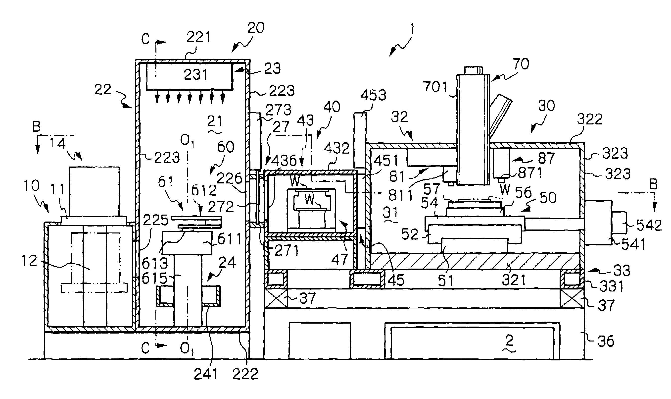
[0147]There will now be described preferred embodiments of the present invention as a substrate inspection apparatus for inspecting a substrate or a wafer as an object to be inspected having a pattern formed on a surface thereof, with reference to the attached drawings.

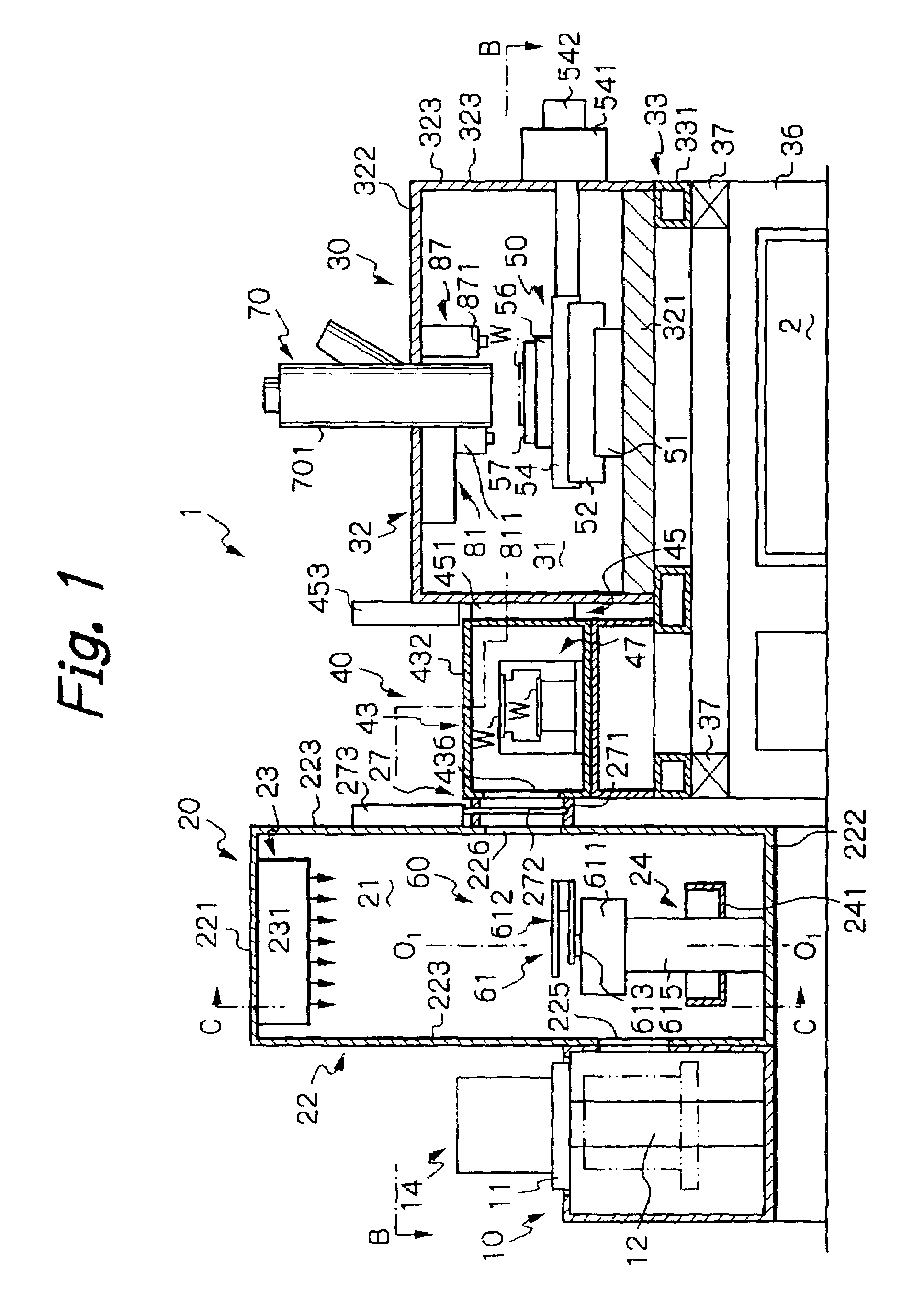
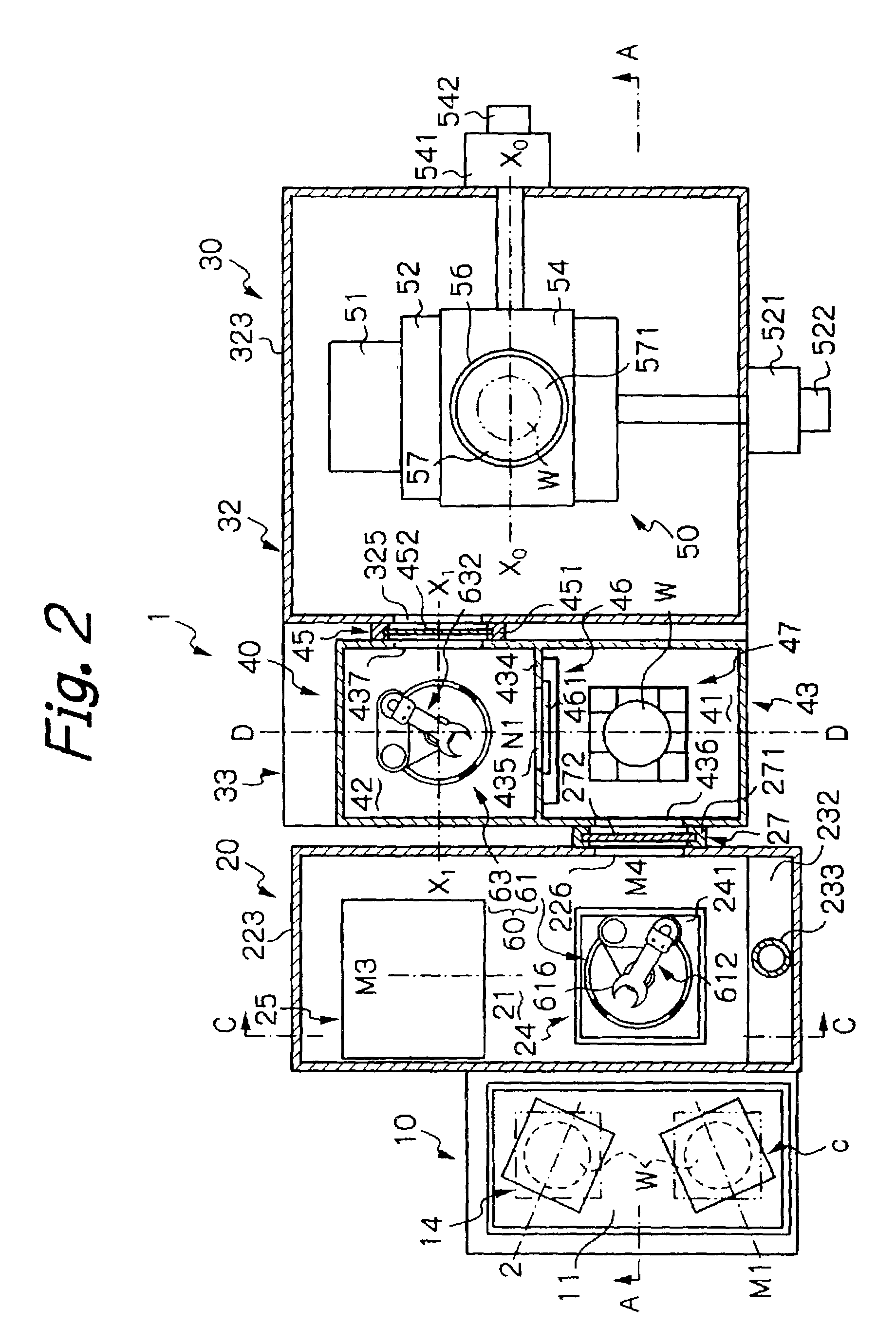
[0148]Referring to FIGS. 1 and 2, main components of a substrate inspection apparatus 1 according to an embodiment of the present invention is shown by an elevational view and a plan view.

[0149]The semiconductor testing apparatus 1 of this embodiment comprises a cassette holder 10 for holding cassettes which stores a plurality of wafers; a mini-environment chamber 20; a main housing 30 which defines a working chamber; a loader housing 40 disposed between the mini-environment chamber 20 and the main housing 30 to define two loading chambers; a loader 60 for loading a wafer from the cassette holder 10 onto a stage device 50 disposed in the main housing 30; and an electro-optical device 70 installed in the vacuum main ho...


PUM


Abstract

The present invention relates to a substrate inspection apparatus for inspecting a pattern formed on a substrate by irradiating a charged particle beam onto the substrate. The substrate inspection apparatus comprises: an electron beam apparatus including a charged particle beam source for emitting a charged particle beam, a primary optical system for irradiating the charged particle beam onto the substrate, a secondary optical system into which a secondary charged particle beam is introduced, the secondary charged particle beam being emitted from the substrate by an irradiation of the charged particle beam, a detection system for detecting the secondary charged particle beam introduced into said secondary optical system and outputting as an electric signal, and a process control system for processing and evaluating the electric signal; a stage unit for holding the substrate and moving the substrate relatively to said electron beam apparatus; a working chamber capable of shielding at least an upper region of the stage unit form outside to control under desired atmosphere; and a substrate load-unload mechanism for transferring the substrate into or out of the stage.

Description

BACKGROUND OF THE INVENTION[0001]In the field of semiconductor processes, the design rule is going into an age of 100 nm and the production form is on a transition from a mass production with a few models representative of a DRAM into a small-lot production with a variety of models such as a SOC (Silicon on chip). This results in an increase of a number of processes, and an improvement in an yield for each process must be essential, which makes more important an inspection for a defect possibly occurring in each process. The present invention relates to a substrate inspection method for inspecting a substrate such as a wafer after respective processes in the semiconductor process by using an electron beam, a substrate inspection apparatus to be used therefor and an electron beam apparatus for the inspection apparatus, and a device manufacturing method using the same method and apparatuses.[0002]In conjunction with a high integration of semiconductor device and a micro-fabrication of...

Claims


Application Information

Patent Timeline
Patent Type & Authority Patents(United States)
IPC IPC(8): H01J37/06G01N23/225H01J37/073H01J37/18H01J37/20H01J37/22H01J37/244H01J37/28
CPCG01N23/225H01J37/073H01J37/185H01J37/20H01J37/222H01J37/244H01J37/28H01J37/06H01J2237/2817H01J2237/082H01J2237/202H01J2237/20228H01J2237/204H01J2237/22H01J2237/24564H01J2237/2806H01J2237/2816
Inventor NAKASUJI, MAMORUNOJI, NOBUHARUSATAKE, TOHRUKIMBA, TOSHIFUMIHATAKEYAMA, MASAHIROWATANABE, KENJISOBUKAWA, HIROSIKARIMATA, TSUTOMUYOSHIKAWA, SHOJIOOWADA, SHINSAITO, MUTSUMIHAMASHIMA, MUNEKI
Owner EBARA CORP
Why Eureka
Try Eureka