Measurement of critical dimensions using X-ray diffraction in reflection mode

a technology of reflection mode and critical dimension, applied in the direction of material analysis using radiation diffraction, measurement devices, instruments, etc., can solve the problems of difficult to precisely control the thickness of the coating on the sidewall, and difficult to measur

Active Publication Date: 2006-09-19
BRUKER TECH LTD
View PDF14 Cites 54 Cited by
  • Summary
  • Abstract
  • Description
  • Claims
  • Application Information

AI Technical Summary

Problems solved by technology

In semiconductor device manufacturing, for example, thin film coatings are commonly deposited over periodic structures of grooves or holes, but the thickness of the coating on the sidewalls is difficult to control precisely and difficult to measure.

Method used


Image

  • Measurement of critical dimensions using X-ray diffraction in reflection mode
  • Measurement of critical dimensions using X-ray diffraction in reflection mode
  • Measurement of critical dimensions using X-ray diffraction in reflection mode

Examples


Embodiment Construction

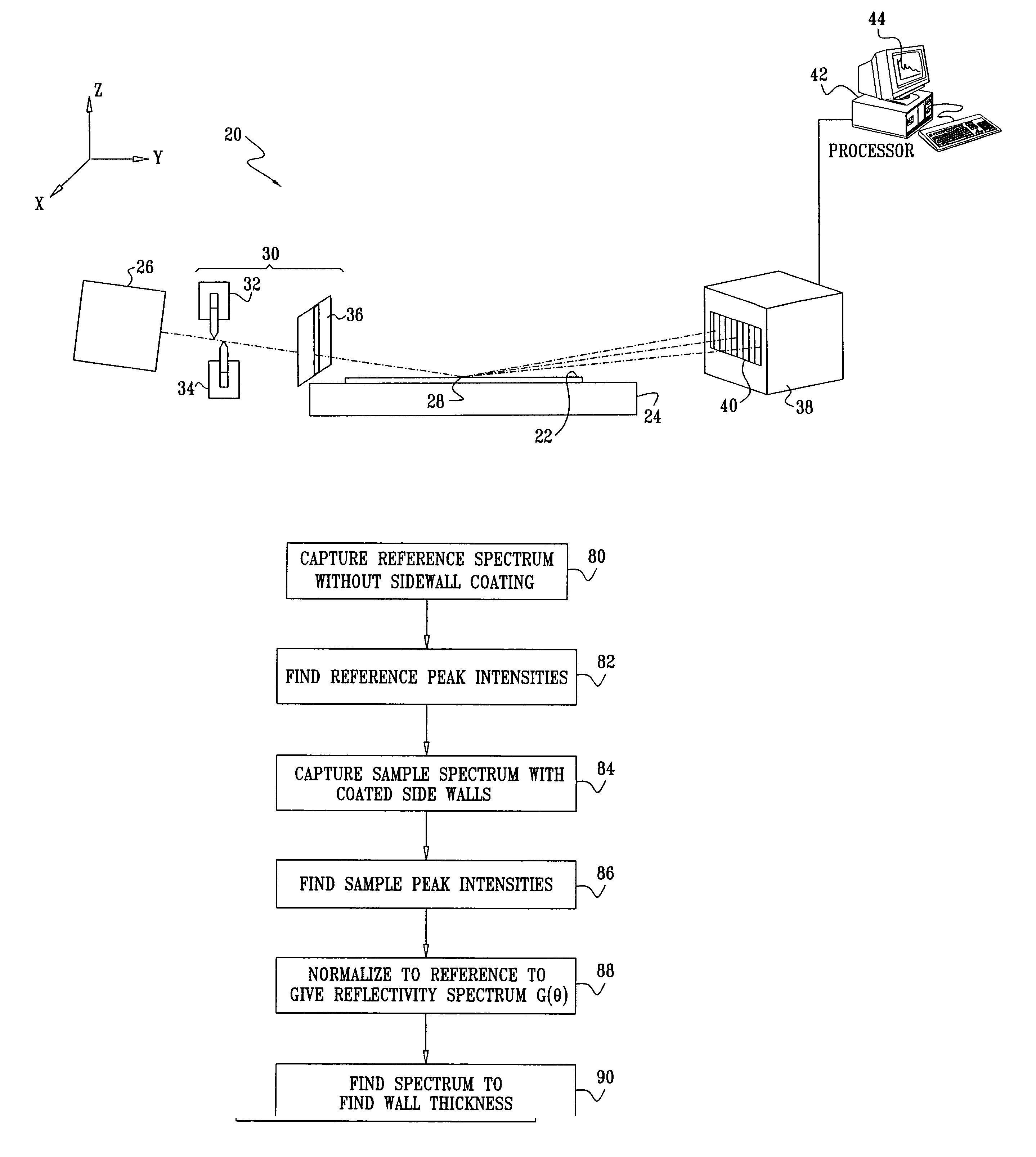
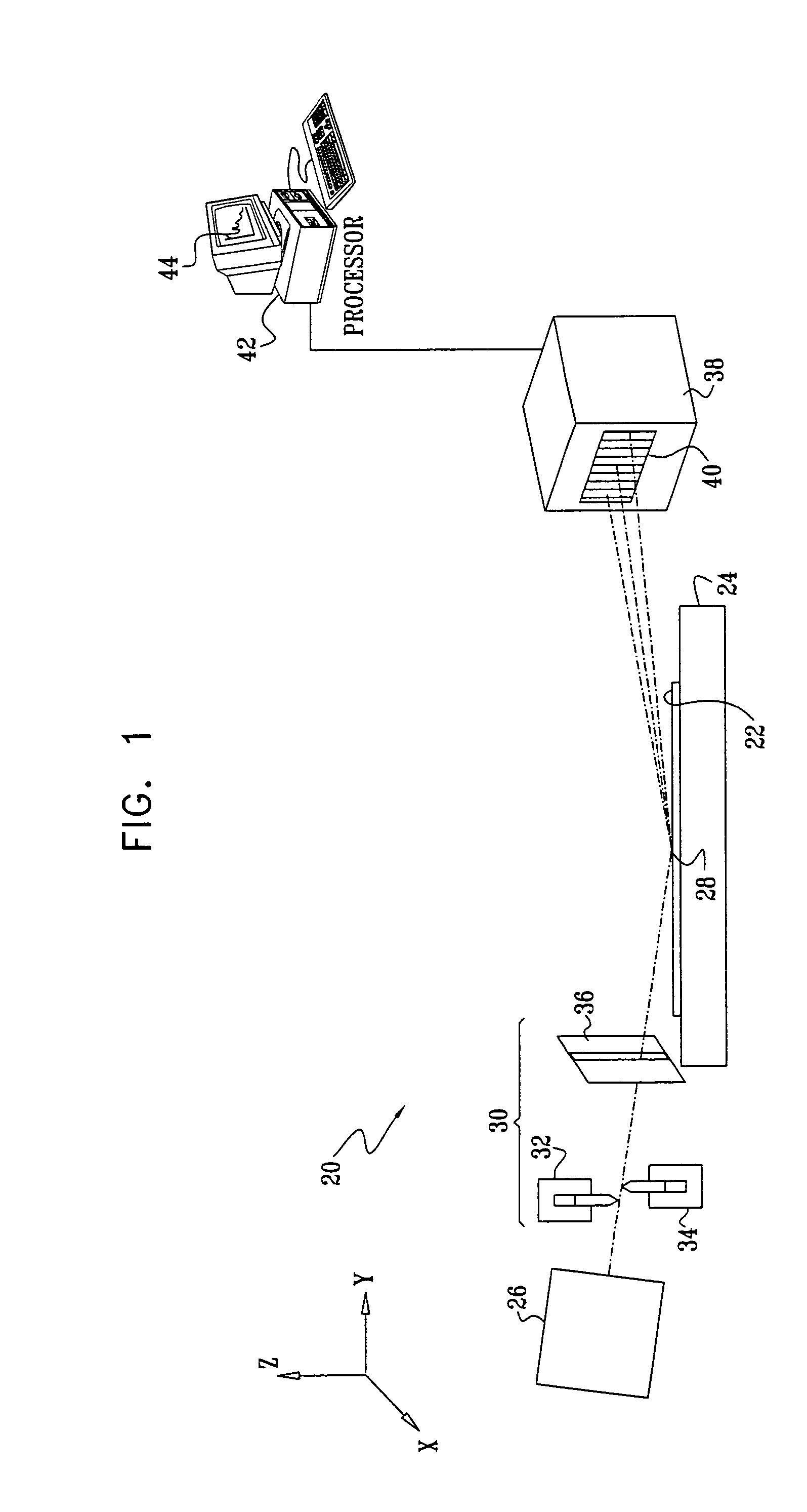
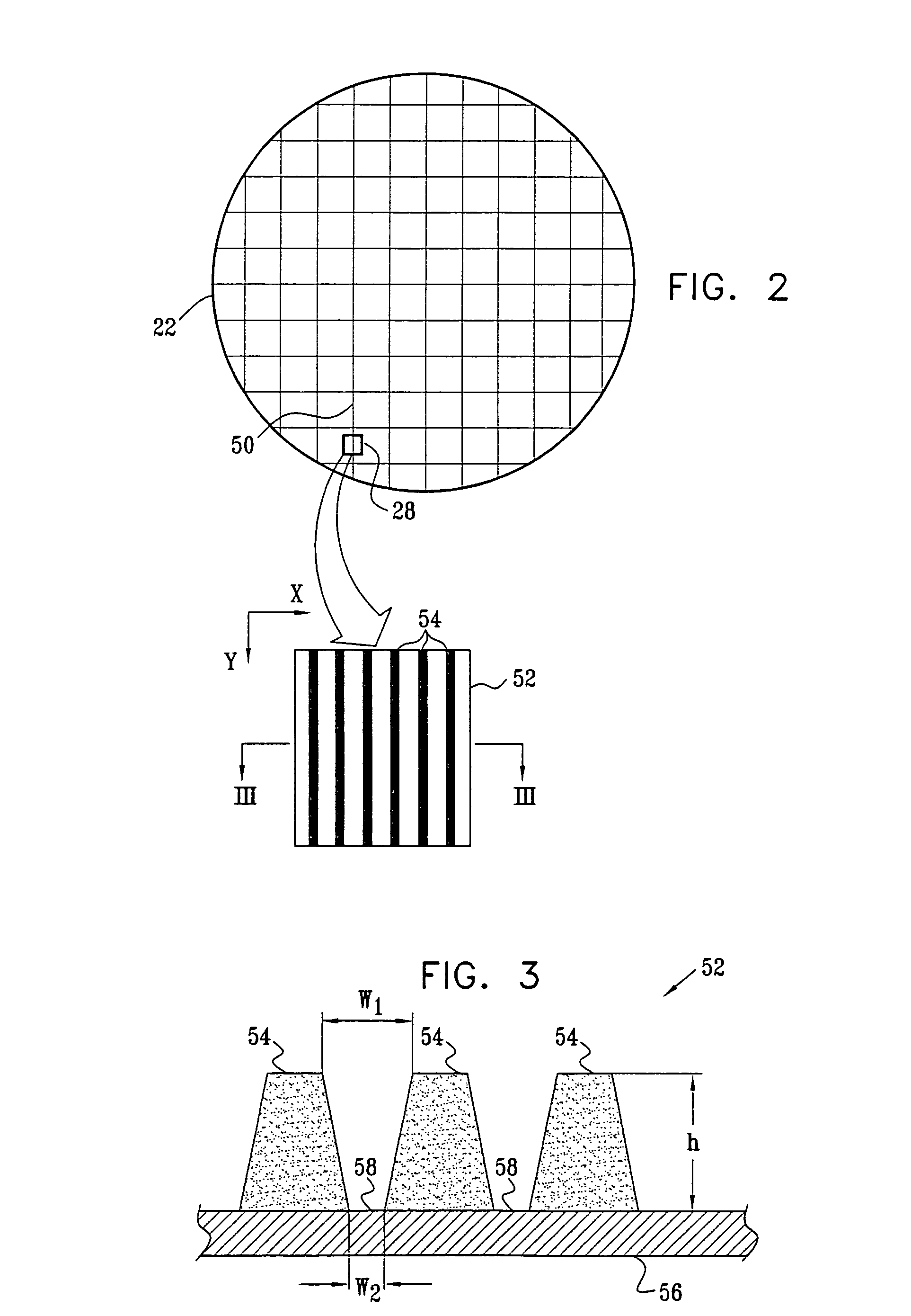
[0054]FIG. 1 is a schematic, pictorial illustration of a system 20 for measurement of critical dimensions on a semiconductor wafer 22, in accordance with an embodiment of the present invention. An X-ray source 26 emits a beam of X-rays, which is collimated by collimating optics 30 and directed onto a target area 28 on wafer 22. The wafer is typically mounted on a motion stage 24, which moves the wafer so that target area 28 may be scanned to different points on the wafer surface. Although the embodiments described hereinbelow relate specifically to wafer 22, the principles of the present invention may similarly be applied to other patterned samples.

[0055]X-ray source 26 typically comprises an X-ray tube with monochromatizing optics (not shown in the figures) For example, the X-ray tube may be an XTF 5011 tube produced by Oxford Instruments, Inc. (Scotts Valley, Calif.). A number of different types of monochromatizing optics that may be used in system 20 are described in U.S. Pat. No...


PUM

PropertyMeasurementUnit
aspect ratioaaaaaaaaaa
incident angleaaaaaaaaaa

Abstract

A method for X-ray analysis of a sample includes directing a beam of X-rays to impinge on an area of a periodic feature on a surface of the sample and receiving the X-rays scattered from the surface in a reflection mode so as to detect a spectrum of diffraction in the scattered X-rays as a function of azimuth. The spectrum of diffraction is analyzed in order to determine a dimension of the feature.

Description

FIELD OF THE INVENTION[0001]The present invention relates generally to semiconductor manufacturing and process control, and specifically to measurements of critical dimensions of semiconductor device features.BACKGROUND OF THE INVENTION[0002]When microelectronic devices are produced on a semiconductor wafer, it is crucial that the critical dimensions of the devices be held within specified tolerances. Critical dimensions, in this context, refer to the widths of features, such as conductors, that are deposited on the wafer and the spacing between adjacent features. Deviations from the specified dimensions lead to performance and yield degradation. The manufacturing process must therefore be carefully monitored and controlled, in order to detect deviations as soon as they occur and to take corrective action to avoid the loss of costly wafers in process. For example, when a critical dimension in photoresist that has been deposited and etched on the wafer is found to be out of specifica...

Claims


Application Information

Patent Timeline
Patent Type & Authority Patents(United States)
IPC IPC(8): G01N23/20
CPCG01N23/20G01N23/207
Inventor MAZOR, ISAACYOKHIN, BORIS
Owner BRUKER TECH LTD
Why Eureka
Try Eureka