

Gate critical dimension variation by use of ghost features
a ghost feature and critical dimension technology, applied in the field of photolithography, can solve the problems of dummy gates interfering with the device performance, the critical dimension (cd) of their corresponding mask approaching the resolution limit of the optical exposure tool, and the inability of current lithography and etching tools and processes
- Summary
- Abstract
- Description
- Claims
- Application Information
AI Technical Summary
Benefits of technology
Problems solved by technology
Method used
Image

Examples
Embodiment Construction
[0001]1. Field of the Invention
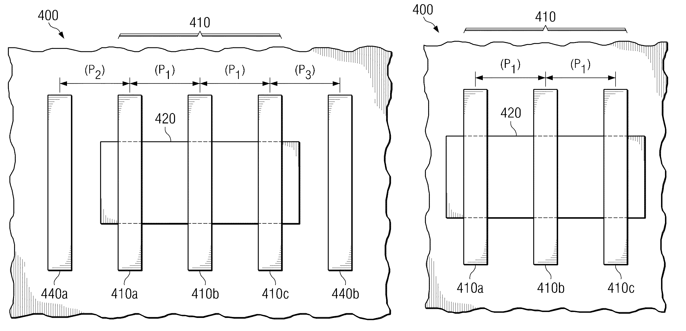
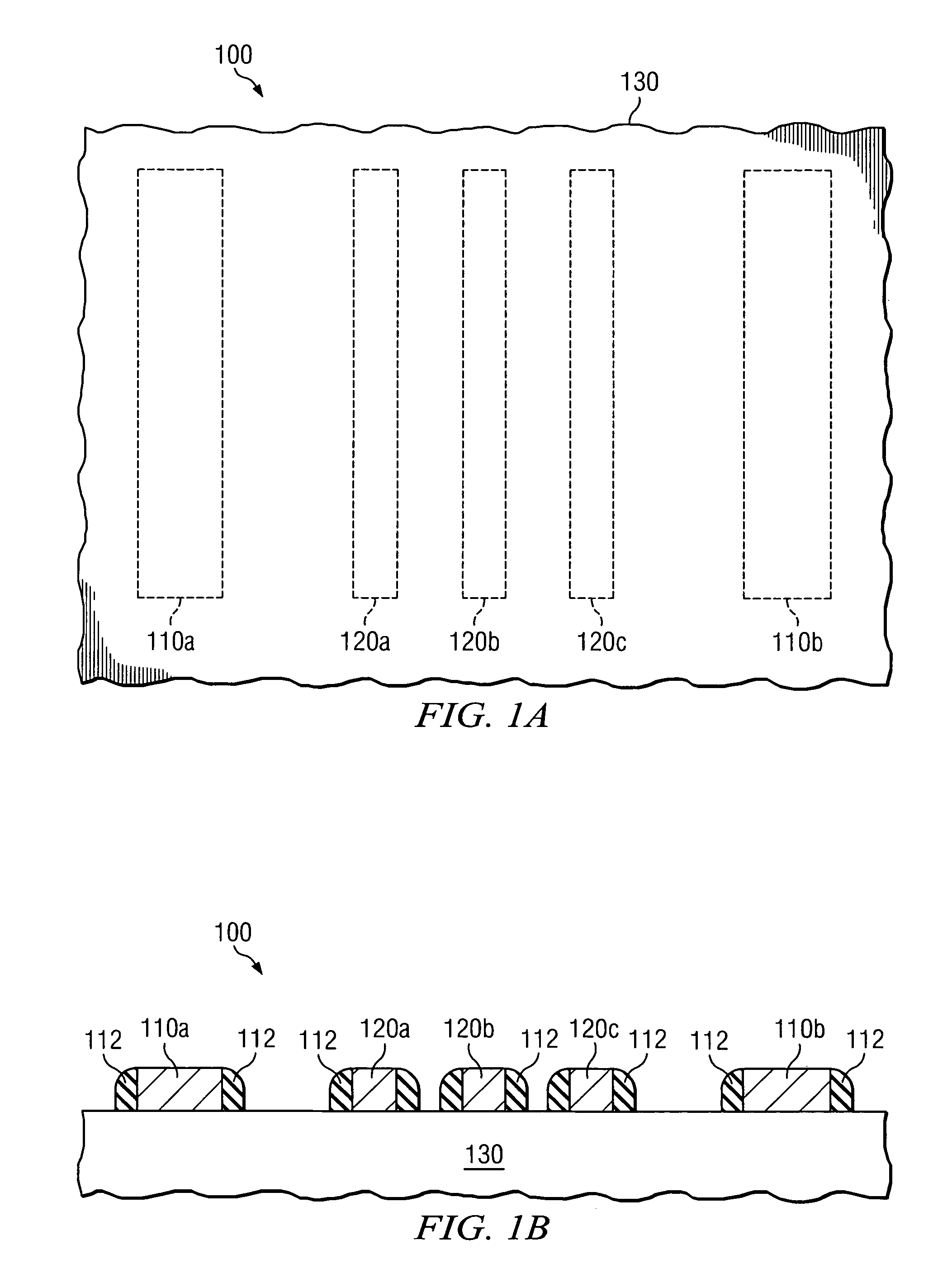
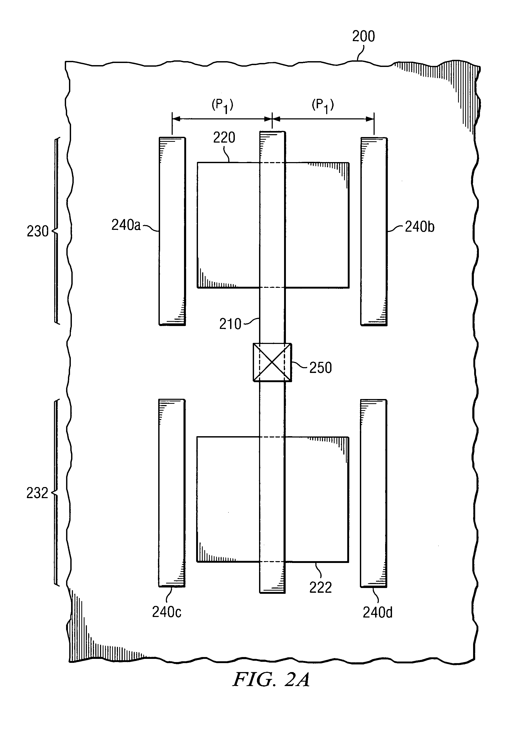
[0002]The subject matter of this invention relates to photolithography for forming integrated circuit devices. More particularly, the subject matter of this application relates to methods and devices used to improve gate critical dimension variation.
[0003]2. Background of the Invention
[0004]Lithographic projection apparatus (tools) can be used, for example, in the manufacture of integrated circuits (ICs). When using the various tools, a mask can be used that contains a circuit pattern corresponding to an individual layer of the IC, and this pattern, usually having many designs, can be imaged onto a target portion (e.g., comprising one or more dies) on a substrate, such as a silicon or other wafer comprising a semiconductor, that has been coated with a layer of radiation-sensitive material, such as a resist. In general, a single wafer may contain a network of adjacent target portions that can be successively irradiated using a projection system of the t...
PUM
| Property | Measurement | Unit |
|---|---|---|
| wavelength | aaaaa | aaaaa |
| wavelength | aaaaa | aaaaa |
| wavelength | aaaaa | aaaaa |
Abstract
Description
Claims
Application Information