Bottom electrode etching process in MRAM cell

a bottom electrode and mram cell technology, applied in the manufacture/treatment of electrical devices, semiconductor devices, electrical apparatus, etc., can solve the problems of limiting the further reduction of line width, affecting the production efficiency of ic devices, and unable to manufacture a very high density ic device as is required for spin torque mram applications

Active Publication Date: 2012-12-18
TAIWAN SEMICON MFG CO LTD
View PDF17 Cites 103 Cited by
  • Summary
  • Abstract
  • Description
  • Claims
  • Application Information

AI Technical Summary

Benefits of technology

[0015]One objective of the present invention is to provide a method of patterning a bottom electrode layer in a MRAM cell such that the MTJ element therein is not damaged by wet and dry process steps during the bottom electrode patterning sequence.
[0016]A second objective of the present invention is to provide a method of patterning a bottom electrode layer in a MRAM cell that essentially eliminates metal residues formed during the patterning sequence thereby substantially reducing BE-BE shorts and BE-BL shorts and improving device yield.
[0020]After RIE etching, the remaining photoresist mask is removed in a wet stripping tool. The cleaning process is another important feature since certain metal residues and metal-photoresist complexes can only be removed by inserting a wet cleaning step before the standard dry cleaning step. Otherwise, a process flow involving a dry stripping step before a first wet stripping causes metal residues (fences) to form that are essentially non-removable by a subsequent wet treatment without damaging the ILD layer. The initial wet clean step with an organic solvent removes the photoresist and typically most of the BARC layer. Preferably, the wet clean is followed by a dry stripping process in a dry plasma chamber to remove any BARC residues. Thereafter, a second wet cleaning step with a water based solution is used to strip any residues formed by plasma etching the residual BARC layer. As a result, adjacent bottom electrodes are well isolated with no BE residues to cause BE-BE shorting and the MTJ is intact and free from plasma etch damage due to the protective dielectric layer. Furthermore, BE residues are stripped by the wet / dry / wet sequence to prevent BE shorting to subsequently deposited bit lines.
[0021]In a second embodiment, a dielectric anti-reflective coating (DARC) which combines the features of an oxide or nitride hard mask with an anti-reflective property is formed on the array of MTJ cells. Thereafter, a photoresist layer is coated on the DARC layer and patterned as in the first embodiment to form an opening between adjacent MTJ cells. Next, a first etch step is performed in a dielectric etch chamber to remove a region of the DARC layer exposed by the opening. The substrate is moved to a metal etch chamber where the BE layer is etched to form a bottom electrode below each MTJ cell. A certain amount of overetch is important to remove BE metal residues that have a tendency to form during the main portion of the BE etch before end point is reached. A wet strip is employed to remove the remaining photoresist layer. In some cases, a thin organic residue may stay on the DARC layer so a dry strip followed by a second wet strip process is preferred to ensure that the DARC surface is clean. The second embodiment represents a cost savings in that fewer process steps are required during the BE patterning sequence.

Problems solved by technology

A sloped profile can not only lead to electrical shorting issues but also limits further reduction of linewidth and makes it impossible to manufacture a very high density IC device as is required for applications such as spin torque MRAM.
As a result, MTJ performance will be degraded.
Another shortcoming of standard MRAM fabrication schemes is that some regions of the ILD may be etched during BE patterning to an extent that the remaining ILD 3 is too thin or penetrated completely thereby damaging an underlying word line.
The method does not teach an overetch treatment of the BE layer to minimize metal residue and does not include a process for removing the photoresist and BARC coatings to avoid defects.

Method used


Image

  • Bottom electrode etching process in MRAM cell
  • Bottom electrode etching process in MRAM cell
  • Bottom electrode etching process in MRAM cell

Examples


Embodiment Construction

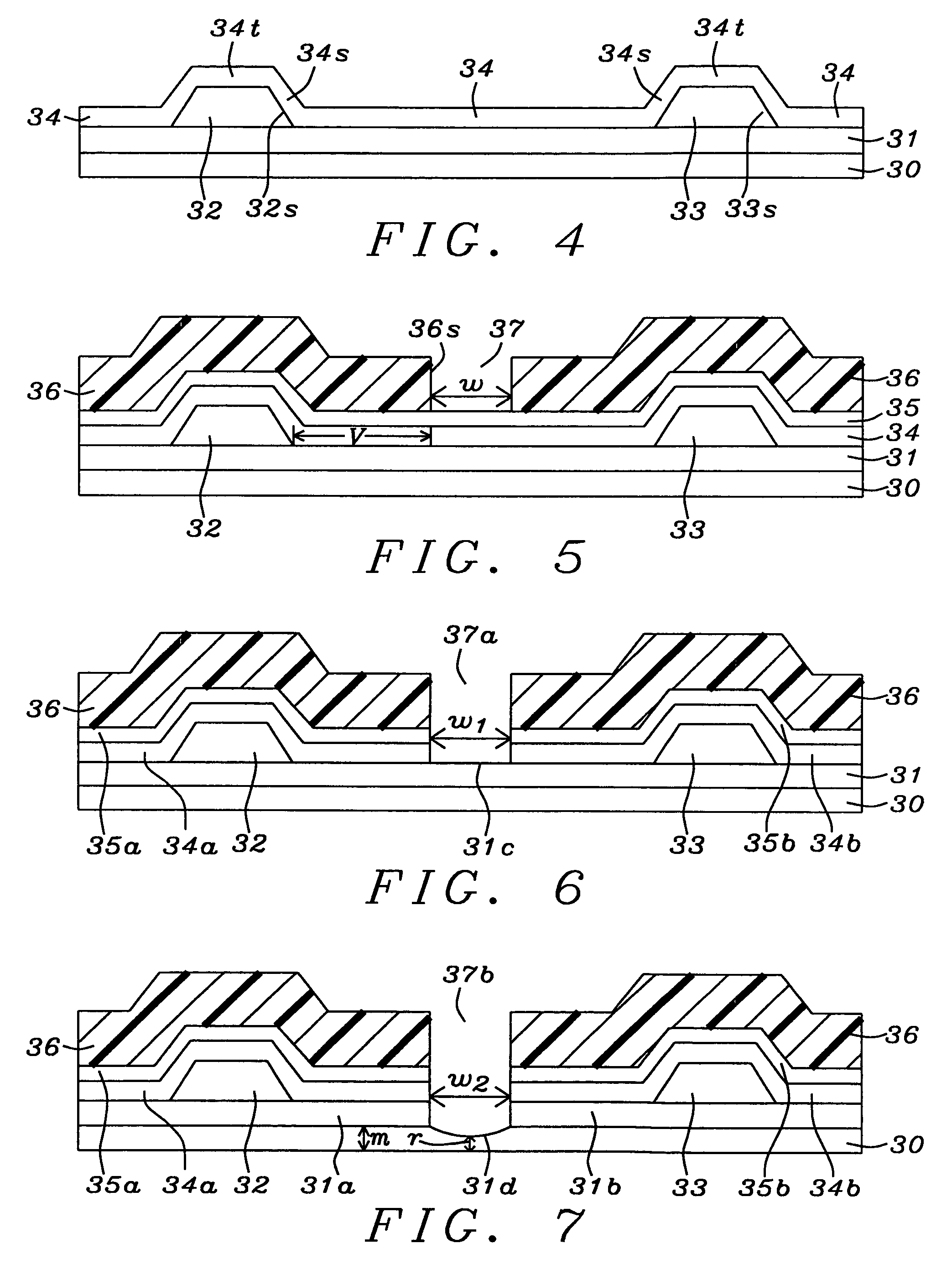
[0029]The present invention is a process sequence for patterning a bottom electrode layer in a MRAM cell that avoids the formation of BE-BE shorts, BE-bit line shorts, and damage to the MTJ element within the MRAM cell. The present invention encompasses various MTJ configurations such as bottom spin valve, top spin valve, and multi-layer spin valve structures. We have found that the BE process sequence is as critical as the selection of materials for various MRAM layers in optimizing device performance.

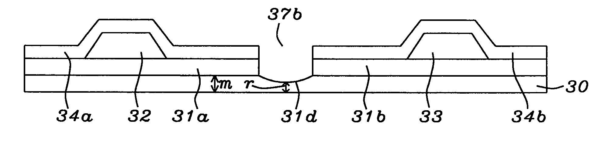
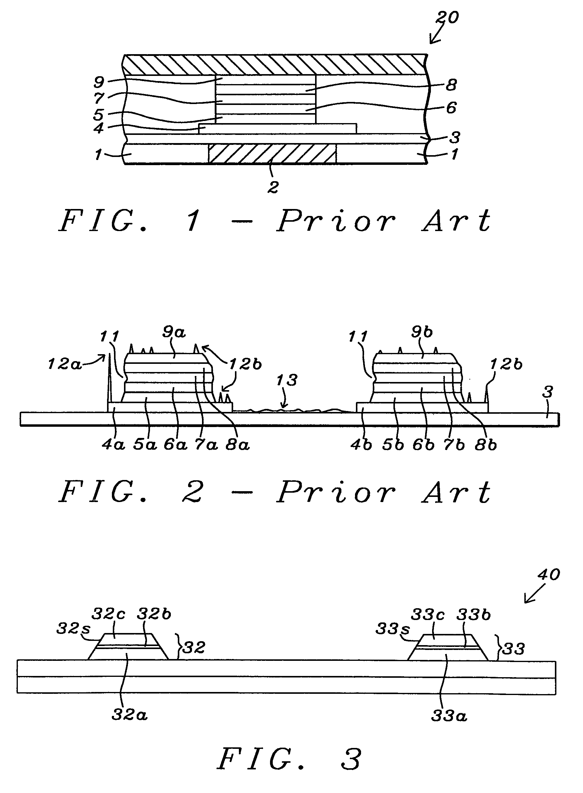
[0030]Referring to FIG. 3, a cross-sectional view of a partially completed MRAM structure 40 is shown that includes two MTJ elements 32, 33 formed on a bottom electrode layer 31, typically with a thickness from 100 to 600 Angstroms. BE layer 31 is disposed on an ILD layer 30 having a thickness in the range of 200 to 800 Angstroms. It should be understood that the MRAM structure 40 comprises a plurality of MTJ elements but only two MTJ elements are depicted in order to simplify the dra...


PUM


Abstract

A BE patterning scheme in a MRAM is disclosed that avoids damage to the MTJ array and underlying ILD layer while reducing BE-BE shorts and BE-bit line shorts. A protective dielectric layer is coated over a MTJ array before a photoresist layer is coated and patterned on the dielectric layer. The photoresist pattern is transferred through the dielectric layer with a dielectric etch process and then through the BE layer with a metal etch that includes a certain amount of overetch to remove metal residues. The photoresist is stripped with a sequence involving immersion or spraying with an organic solution followed by oxygen ashing to remove any other organic materials. Finally, a second wet strip is performed with a water based solution to provide a residue free substrate. In another embodiment, a bottom anti-reflective coating (BARC) is inserted between the photoresist and dielectric layer for improved critical dimension control.

Description

RELATED PATENT APPLICATION[0001]This application is related to the following: U.S. Patent Application Publication 2008 / 0090307; and U.S. Patent Application Publication 2009 / 0078927, both assigned to a common assignee and herein incorporated by reference in their entirety.FIELD OF THE INVENTION[0002]The invention relates to a method of patterning a bottom electrode (BE) during fabrication of a MRAM cell, and in particular to a process sequence that eliminates BE-BE shorts, BE-bit line shorts, and prevents damage to magnetic tunnel junction (MTJ) sidewalls during etching and cleaning steps.BACKGROUND OF THE INVENTION[0003]Magnetoresistive Random Access Memory (MRAM), based on the integration of silicon CMOS with MTJ technology, is a major emerging technology that is highly competitive with existing semiconductor memories such as SRAM, DRAM, Flash, etc. A MRAM device is generally comprised of an array of parallel first conductive lines on a horizontal plane, an array of parallel second...

Claims


Application Information

Patent Timeline
Patent Type & Authority Patents(United States)
IPC IPC(8): H01L21/302B44C1/22
CPCH01L27/222H01L43/12H10B61/00H10N50/01
Inventor MAO, GUOMIN
Owner TAIWAN SEMICON MFG CO LTD
Why Eureka
Try Eureka