Methods and systems for determining a critical dimension, a presence of defects, and a thin film characteristic of a specimen

a technology of critical dimension and specimen, applied in the direction of semiconductor/solid-state device testing/measurement, instruments, fluorescence/phosphorescence, etc., can solve the problems of non-uniformity, semiconductor fabrication process may introduce a number of defects, and semiconductor fabrication process is among the most sophisticated and complex processes used in manufacturing

Inactive Publication Date: 2005-07-19
KLA TENCOR TECH CORP
View PDF331 Cites 110 Cited by
  • Summary
  • Abstract
  • Description
  • Claims
  • Application Information

AI Technical Summary

Benefits of technology

[0097]In an embodiment, the processor may include a local processor coupled to the beam profile ellipsometer and/or the etch tool and a remote controller computer coupled to the local processor. The local processor may be configured to at least partially process the one or more output signals. The remote controller computer may be configured to receive the at least partially processed one or more output signals from the processor. In addition, the remote controller computer may be configured to determine a property of an etched region on the specimen from the at least partially processed one or

Problems solved by technology

Semiconductor fabrication processes, however, are among the most sophisticated and complex processes used in manufacturing.
For example, semiconductor fabrication processes may introduce a number of defects (e.g., non-uniformities) into a semiconductor device.
As an example, defects may include contamination introduced to a wafer during a semiconductor fabrication process by particles in process chemicals and/or in a clean room environment.
Such defects may adversely affect the performance of the process to an extent that overall yield of the fabrication process may be reduced below acceptable levels.
As features sizes of semiconductor devices continue to shrink, a minimum feature size that may be fabricated may often be limited by the performance characteristics of a semiconductor fabrication process.
In optical lithography, for example, performance characteristics such as resolution capability of a lithography process may be limited by the quality of the resist application, the performance of the resist material, the performance of the exposure tool, and the wavelength of light used to expose the resist.
There are several disadvantages, however, in using the currently available methods and systems for metrology and/or inspection of specimens fabricated by semiconductor fabrication processes.
Multiple metrology/inspection systems, however, may occupy a relatively large amount of clean room space due to the footprints of each of the metrology and/or inspection systems.
In addition, testing time and process delays associated with measuring and/or inspecting a specimen with multiple metrology/inspection systems may increase the overall cost of manufacturing and the manufacturing time for fabricating a semiconductor device.
For example, process tools may often be idle while metrology and/or inspection of a spe

Method used


Image

  • Methods and systems for determining a critical dimension, a presence of defects, and a thin film characteristic of a specimen
  • Methods and systems for determining a critical dimension, a presence of defects, and a thin film characteristic of a specimen
  • Methods and systems for determining a critical dimension, a presence of defects, and a thin film characteristic of a specimen

Examples


Embodiment Construction

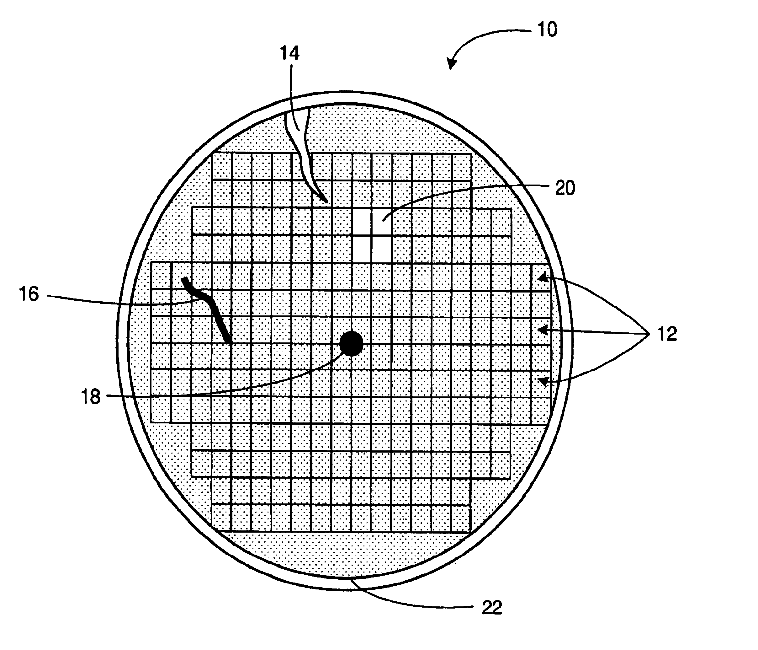
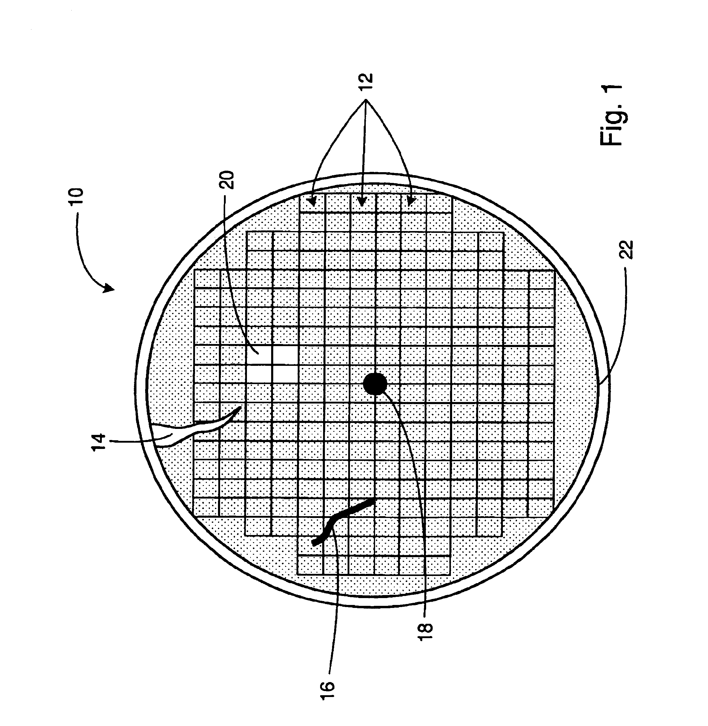
[0157]Turning now to the drawings, FIG. 1 illustrates a schematic top view of an embodiment of a surface of specimen 10. Specimen 10 may include a substrate such as a monocrystalline silicon substrate, a silicon germanium substrate, or a gallium arsenide substrate. In addition, specimen 10 may include any substrate suitable for fabrication of semiconductor devices. Specimen 10 may include plurality of dies 12 having repeatable pattern features. Alternatively, specimen 10 may be unpatterned such as a virgin semiconductor wafer or an unprocessed wafer. In addition, specimen 10 may include a glass substrate or any substrate formed from a substantially transparent material, which may be suitable for fabrication of a reticle. Furthermore, specimen 10 may include any specimen known in the art.

[0158]In addition, specimen 10 may include one or more layers arranged upon a substrate. For example, layers which may be formed on a substrate may include, but are not limited to, a resist, a dielec...


PUM


Abstract

Methods and systems for monitoring semiconductor fabrication processes are provided. A system may include a stage configured to support a specimen and coupled to a measurement device. The measurement device may include an illumination system and a detection system. The illumination system and the detection system may be configured such that the system may be configured to determine multiple properties of the specimen. For example, the system may be configured to determine multiple properties of a specimen including, but not limited to, critical dimension, a presence of defects, and a thin film characteristic. In this manner, a measurement device may perform multiple optical and/or non-optical metrology and/or inspection techniques.

Description

PRIORITY CLAIM[0001]This application claims priority to U.S. Provisional Application No. 60 / 234,323 entitled “Methods and Systems for Semiconductor Fabrication Processes,” filed Sep. 20, 2000.BACKGROUND OF THE INVENTION[0002]1. Field of the Invention[0003]This invention generally relates to methods and systems for semiconductor fabrication processes. Certain embodiments relate to a method and a system for evaluating and / or controlling a semiconductor fabrication process by determining at least two properties of a specimen.[0004]2. Description of the Related Art[0005]Fabrication of semiconductor devices such as logic and memory devices typically includes a number of processes that may be used to form various features and multiple levels or layers of semiconductor devices on a surface of a semiconductor wafer or another appropriate substrate. For example, lithography is a process that typically involves transferring a pattern to a resist arranged on a surface of a semiconductor wafer....

Claims


Application Information

Patent Timeline
IPC IPC(8): G01N21/64G01N21/47G01N21/21G01N21/63G01N21/88G01N21/95G03F7/20H01L21/66
CPCG03F7/70625G03F7/70633G03F7/7065G03F7/70658G03F7/707G03F7/70708G01N21/211G01N21/4788G01N21/636G01N21/64G01N21/9501G03F7/70616H01L2924/0002H01J2237/31701H01L22/12G01N2021/646G01N2021/8825H01L2924/00
Inventor NIKOONAHAD, MEHRDADLEVY, ADYBROWN, KYLE A.BULTMAN, GARYWACK, DANFIELDEN, JOHN
Owner KLA TENCOR TECH CORP
Why Eureka
Try Eureka