Solders with surfactant-refined grain sizes, solder bumps made thereof, and methods of making same

a technology of surfactant and grain size, which is applied in the direction of soldering apparatus, semiconductor/solid-state device details, manufacturing tools, etc., can solve the problems of thermal expansion cracking of ild materials, weak and brittle ild materials, and integration problems

Inactive Publication Date: 2006-09-26
INTEL CORP
View PDF18 Cites 11 Cited by
  • Summary
  • Abstract
  • Description
  • Claims
  • Application Information

AI Technical Summary

Problems solved by technology

The relatively weak and brittle ILD material gives rise to integration problems, where the packaged die is attached to a moun

Method used


Image

  • Solders with surfactant-refined grain sizes, solder bumps made thereof, and methods of making same
  • Solders with surfactant-refined grain sizes, solder bumps made thereof, and methods of making same
  • Solders with surfactant-refined grain sizes, solder bumps made thereof, and methods of making same

Examples


Embodiment Construction

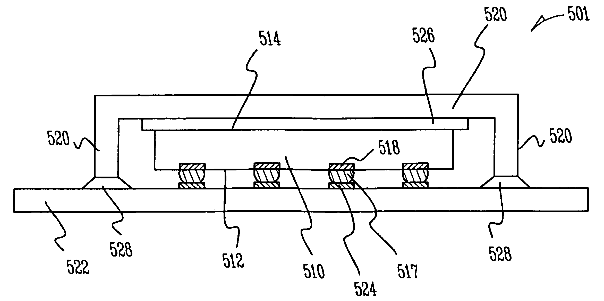
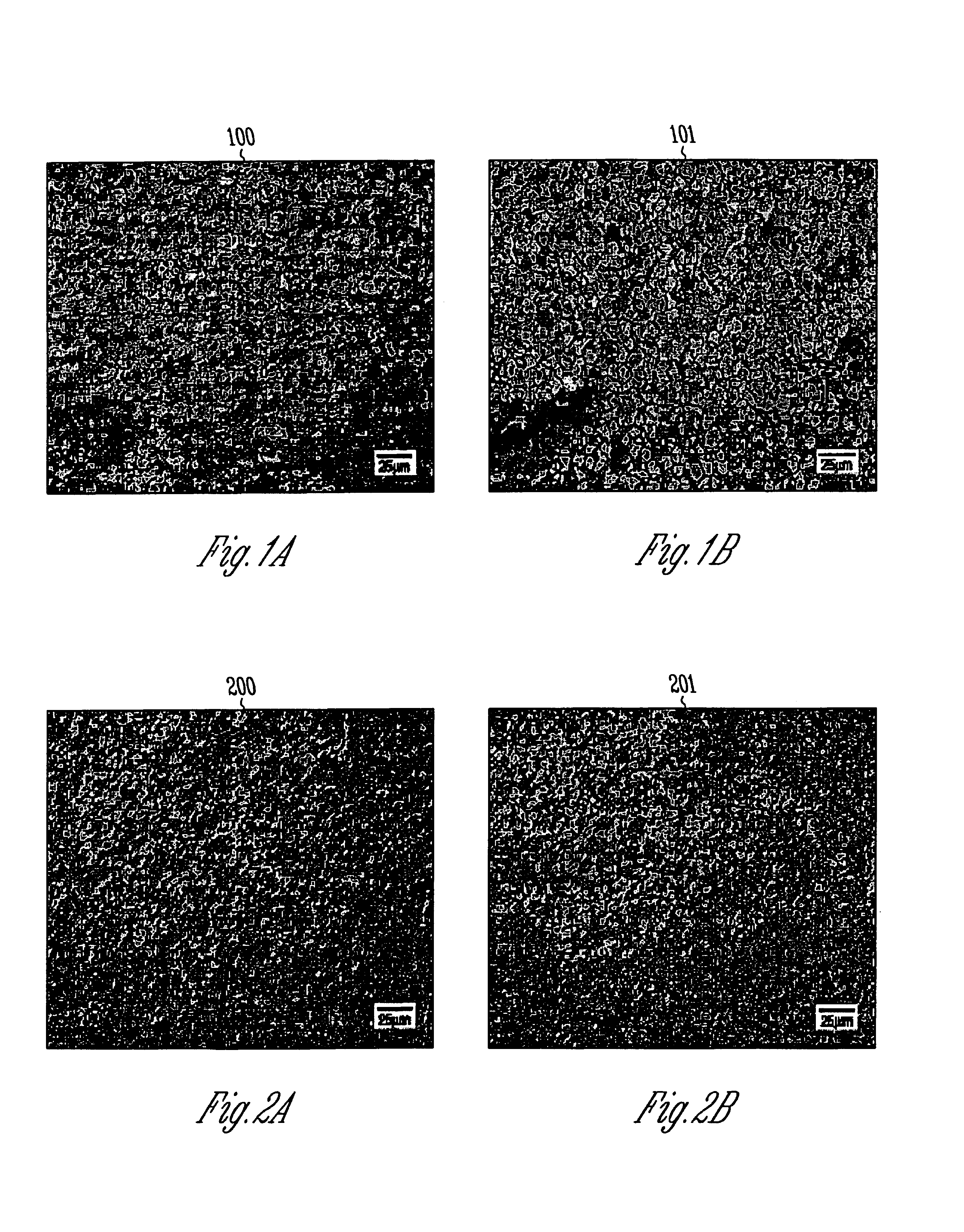
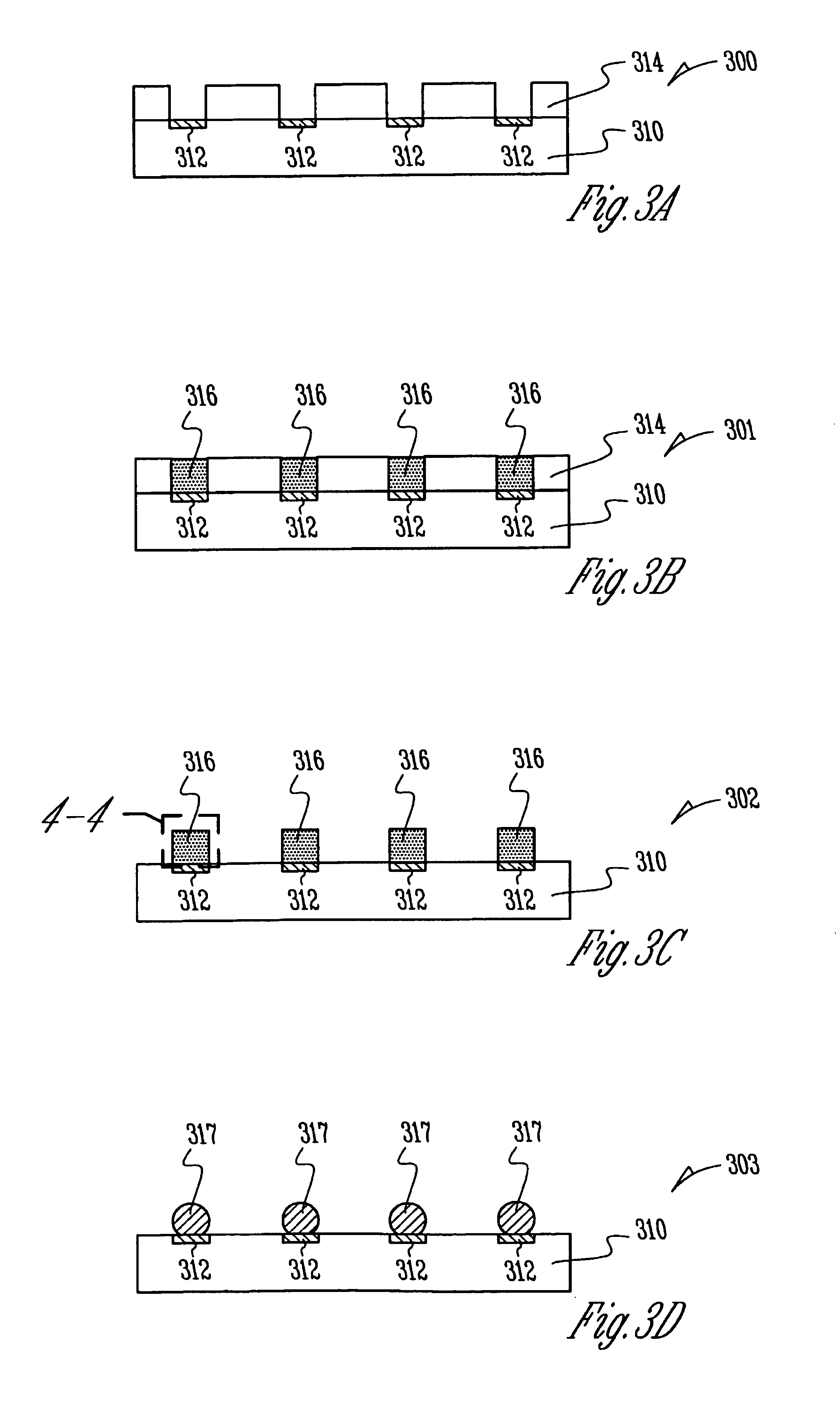
[0019]The following description includes terms, such as upper, lower, first, second, etc., that are used for descriptive purposes only and are not to be construed as limiting. The embodiments of a device or article described herein can be manufactured, used, or shipped in a number of positions and orientations. The terms “die” and “processor” generally refer to the physical object that is the basic workpiece that is transformed by various process operations into the desired integrated circuit device. A board is typically a resin-impregnated fiberglass structure that acts as a mounting substrate for the die. A die is usually singulated from a wafer, and wafers may be made of semiconducting, non-semiconducting, or combinations of semiconducting and non-semiconducting materials.

[0020]Reference will now be made to the drawings wherein like structures will be provided with like reference designations. In order to show the structure and process embodiments most clearly, the drawings inclu...


PUM

PropertyMeasurementUnit
Grain sizeaaaaaaaaaa

Abstract

A doped tin-indium solder composition is disclosed. The doped tin-indium solder exhibits a retained fine-grain structure and superplasticity after significant thermal cycling and thermal and mechanical stresses experienced in a microelectronic package. A process of forming the doped tin-indium solder is also disclosed. A microelectronic package is also disclosed that uses the doped tin-indium solder composition. A method of assembling a microelectronic package is also disclosed. A computing system is also disclosed that includes the doped tin-indium solder.

Description

TECHNICAL FIELD[0001]Disclosed embodiments relate to a refined grain size solder for use in a microelectronic device package. The refined grain size solder can exhibit superplastic behavior during ordinary thermal cycling of the microelectronic device package.BACKGROUND INFORMATIONDescription of Related Art[0002]An integrated circuit (IC) die is often fabricated into a processor for various tasks. Increased speed in an IC die has required one die-fabricating path to include an interlayer dielectric layer (ILD) to have properties that are relatively weak and brittle with respect to the metallization of the die. The relatively weak and brittle ILD material gives rise to integration problems, where the packaged die is attached to a mounting substrate. Machine operation also causes the ILD materials to crack from thermal expansion stresses, among other reasons.[0003]One problem that must be addressed in the connection of various different types of materials (i.e., microelectronic device...

Claims


Application Information

Patent Timeline
IPC IPC(8): B23K31/02C22C13/02H01L23/48B23K35/02B23K35/14B23K35/26H01L21/60H01L23/485H05K3/34
CPCB23K35/262H01L24/11H01L24/81H01L24/13B23K35/0227B23K35/0233H01L2924/014B23K35/0244H01L2224/1147H01L2224/13099H01L2224/13147H01L2224/16H01L2224/73253H01L2224/81801H01L2924/01013H01L2924/01029H01L2924/0103H01L2924/01032H01L2924/01047H01L2924/01049H01L2924/01051H01L2924/01052H01L2924/01078H01L2924/01082H01L2924/01322H01L2924/14H01L2924/1433H01L2924/16152H05K3/3436H05K3/3463H01L2924/01005H01L2924/01006H01L2924/0105H01L2924/351H01L2224/05571H01L2224/05573H01L2924/00014H01L2924/00H01L2224/05599
Inventor HUA, FAY
Owner INTEL CORP
Why Eureka
Try Eureka