Method of manufacturing semiconductor device

a manufacturing method and technology for semiconductor devices, applied in the direction of semiconductor devices, basic electric elements, electrical equipment, etc., can solve the problems of difficult to peel off the chips of non-ultraviolet curing type adhesive tape, and reducing the adhesive strength

Active Publication Date: 2006-10-03
RENESAS EASTERN JAPAN SEMICON INC +1
View PDF2 Cites 52 Cited by
  • Summary
  • Abstract
  • Description
  • Claims
  • Application Information

AI Technical Summary

Benefits of technology

[0023]At the time of peeling off the respective semiconductor chips from the adhesive tape after dividing the plurality of semiconductor chips by dicing the semiconductor wafer laminated to a UV curing type tape or a non-UV curing type tape, even when the chips are extremely thin, it is possible to peel off these chips without generating cracks and chippings.

Problems solved by technology

However, the ultraviolet (UV) curing type adhesive tape has a disadvantage in that it is costly compared to the non-ultraviolet (UV) curing type adhesive tape.
However, in contrast to the ultraviolet (UV) curing type adhesive tape, it is impossible reduce the adhesive strength of the non-ultraviolet (UV) curing type adhesive tape by curing the adhesive, and, hence, it is difficult to peel chips off of the non-ultraviolet (UV) curing type adhesive tape compared to the ultraviolet (UV) curing type adhesive tape.
That is, even when the peeling-off of the chips is attempted by pushing a pusher pin provided with a large number of needles against the back surface of the adhesive tape, the peeling-off operation requires a considerable time.
Alternatively, when thin chips are adopted, the chips cannot withstand a bending stress and will tend to crack.

Method used


Image

  • Method of manufacturing semiconductor device
  • Method of manufacturing semiconductor device
  • Method of manufacturing semiconductor device

Examples


embodiment 1

(Embodiment 1)

[0073]This embodiment is applied to the manufacture of a semiconductor package which mounts chips on a printed circuit wiring board. A method of manufacture of the semiconductor package will be explained in the order of the steps thereof in conjunction with FIG. 1 to FIG. 25.

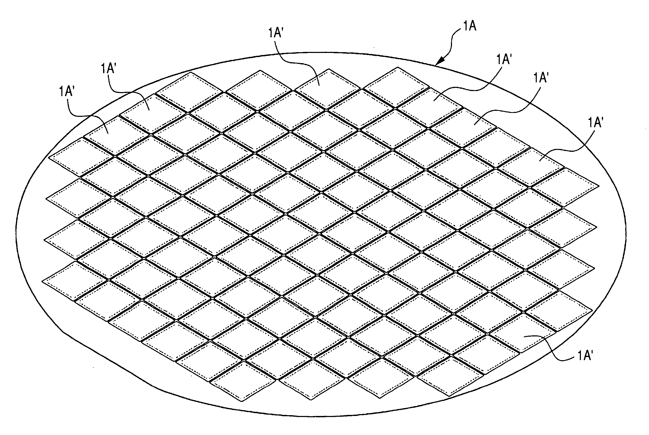
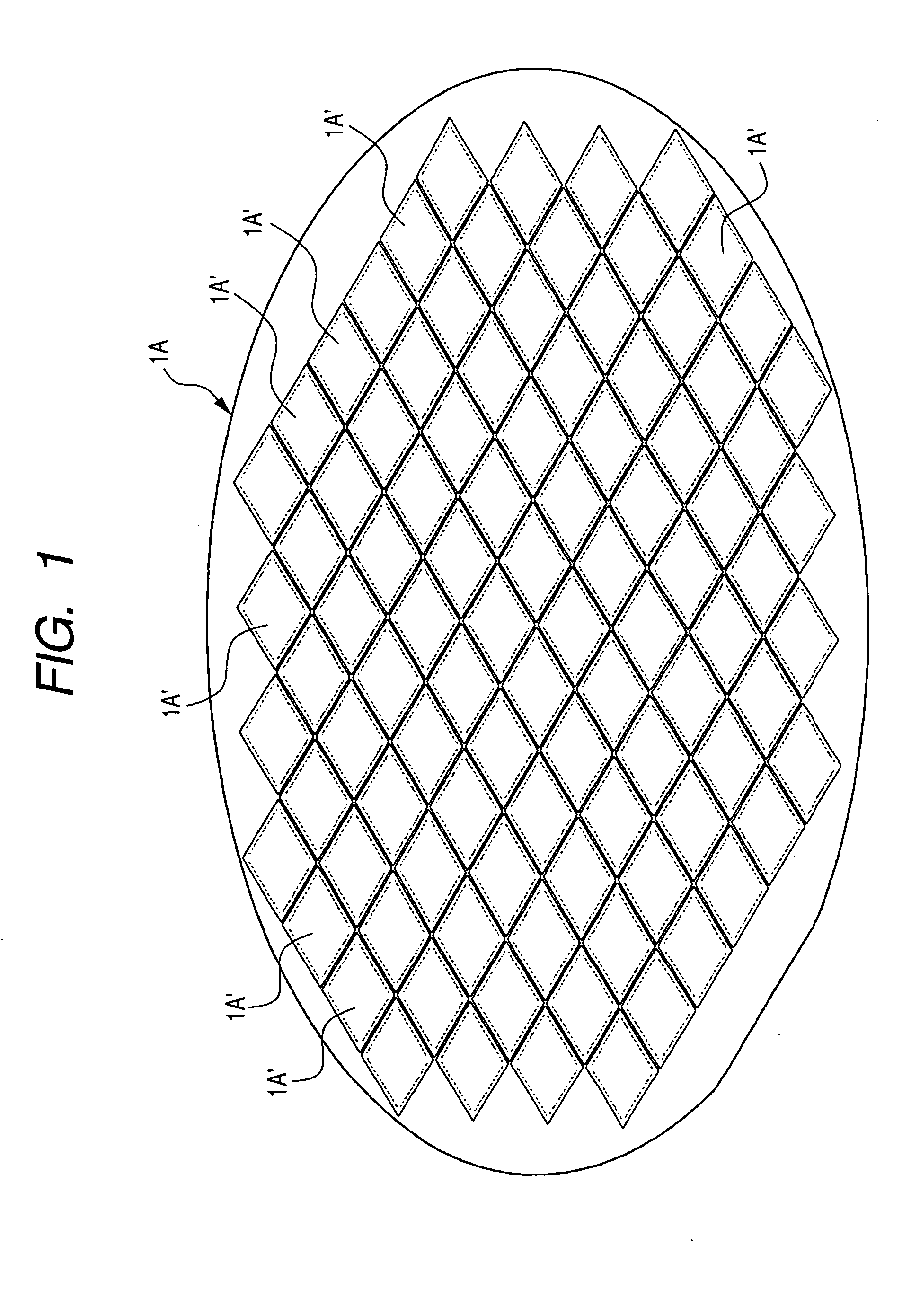
[0074]First of all, an integrated circuit is formed over a main surface of a wafer 1A made of single crystal silicon, as shown in FIG. 1, in accordance with a well-known manufacturing process; and, thereafter, an electric test is performed on integrated circuits which are respectively formed on a plurality of chip forming regions 1A′, which are defined by grid-like scribe lines, so as to judge whether respective chip forming regions 1A′ are defective or non-defective. The chip forming region 1A′ used in this embodiment has a square planar shape, with longitudinal and lateral lengths which are equal.

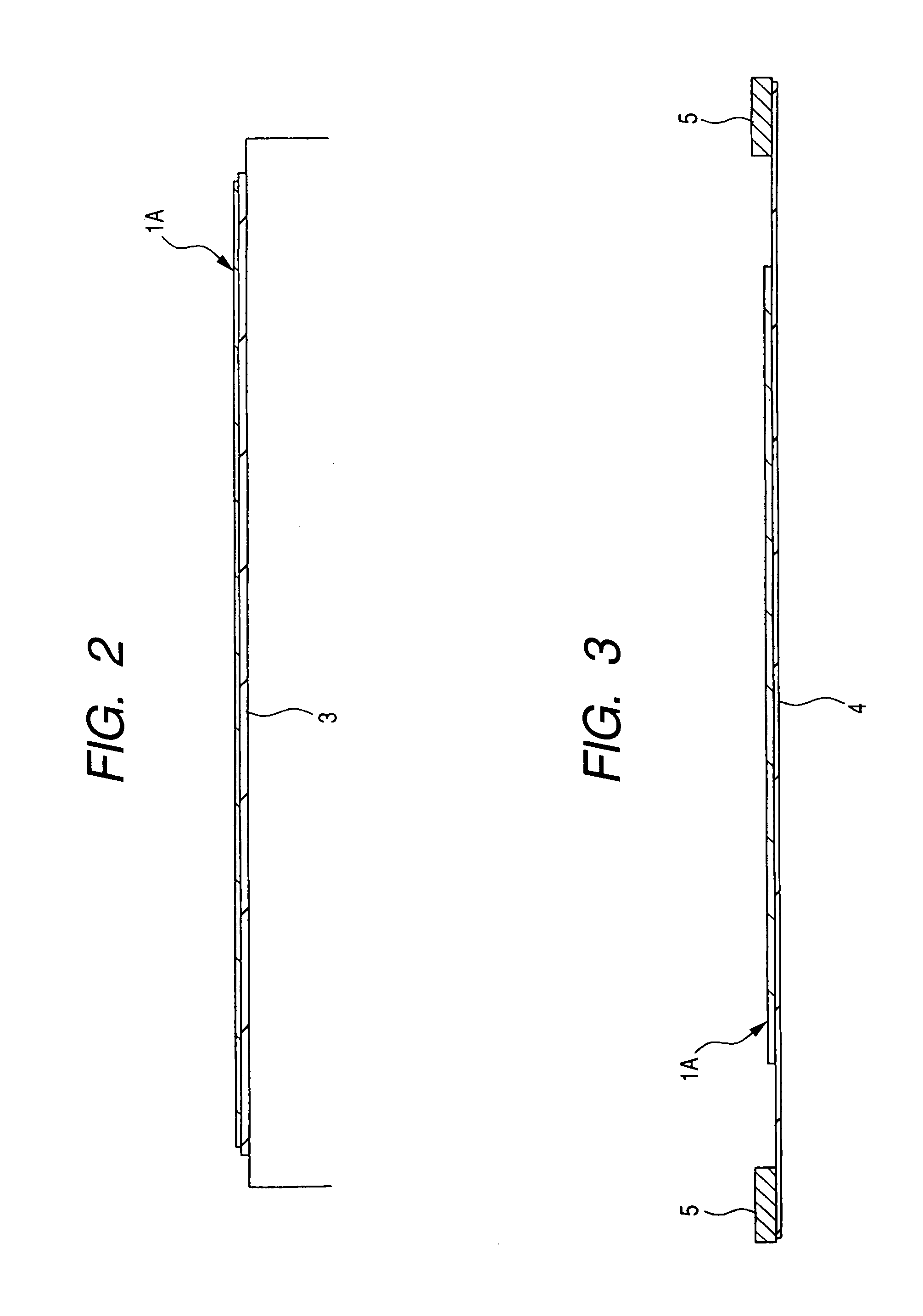
[0075]Next, as shown in FIG. 2, a back grind tape 3 for protecting the integrated circuit is laminate...

embodiment 2

(Embodiment 2)

[0113]The above-mentioned embodiment 1 adopts a method in which, first of all, three blocks 110a to 110c are simultaneously pushed upwardly, and, thereafter, the intermediate block 110b and the inner block 110c are further pushed up, and, finally, the inner block 110c is further pushed upwardly so as to peel off the chip 1 from the dicing tape 4.

[0114]On the contrary, as shown in FIG. 28, first of all, three blocks 110a to 110c are simultaneously pushed upwardly so as to uniformly peel off the whole peripheral portion of the chip 1 from the dicing tape 4, and, thereafter, as shown in FIG. 29, the outer block 110a is lowered to cause the peeling of the chip 1 from the dicing tape 4 to progress in a direction toward the center of the chip 1. Then, as a final step, as shown in FIG. 30, the intermediate block 110b is lowered to further cause the peeling of the chip 1 from the dicing tape 4 to progress in the direction toward the center of the chip 1, so as to completely pe...

embodiment 3

(Embodiment 3)

[0117]The above-mentioned embodiment 1 has been directed to a case in which the chip 1 which represents the object to be peeled off has a square shape. However, to peel off a rectangular chip 1 having longitudinal and lateral lengths which differ from each other, for example, as shown in FIG. 31, three rectangular blocks 210a to 210c which differ in size are used. Due to such a constitution, it is possible to efficiently cause the peeling to progress by focusing the stress on the peeling start point of the chip 1 and the dicing tape 4, while reducing the bending stress applied to the chip 1. Here, as the outer block 210a having the largest diameter, it is preferable to use a block having a diameter slightly smaller than the chip 1 which represents the object to be peeled, thus preventing a strong load from being applied to the outermost portion of the chip 1.

[0118]To peel off the chip 1 using the rectangular blocks 210a to 210c, first of all, as shown in FIG. 32(a), th...


PUM


Abstract

Extremely thin chips laminated to a non-ultraviolet ray curing type adhesive tape are peeled from the tape without giving rise to cracks and chippings. In a center portion of a suction block used for peeling off a chip laminated to a dicing tape, three blocks which push the dicing tape upwardly are incorporated. With respect to these blocks, inside the first block having a largest diameter, there is a second block having a diameter smaller than the diameter of the first block. Further, inside the second block, there is a third block having the smallest diameter. To peel off a chip by pushing a back surface of the dicing tape with the blocks, first of all, the three blocks are simultaneously pushed upwardly by a certain amount and, thereafter, the intermediate block and the inner block are further pushed upward, and, finally, the inner block is further pushed upward.

Description

CROSS-REFERENCE TO RELATED APPLICATION[0001]The present application claims priority from Japanese patent application JP 2003-324838, filed on Sep. 17, 2003, the content of which is hereby incorporated by reference into this application.BACKGROUND OF THE INVENTION[0002]The present invention relates to a technique for use in the manufacture of a semiconductor device, and, more particularly, to a technique which is effective when applied to steps in which a semiconductor wafer adhered to an adhesive tape is divided into a plurality of semiconductor chips by dicing, and, thereafter, the respective semiconductor chips are peeled off from the adhesive tape.[0003]Recently, with a view toward enhancement of high-density packaging of a semiconductor device, a stacked package which three-dimensionally mounts plural sheets of semiconductor chips on a printed circuit wiring board has been put into practice. However, in assembling such a stacked package, semiconductor chips (hereinafter, simply ...

Claims


Application Information

Patent Timeline
Patent Type & Authority Patents(United States)
IPC IPC(8): H01L21/30H01L21/67H01L21/00H01L21/301H01L21/50H01L21/52H01L21/68H01L21/683H01L21/78
CPCH01L21/67132H01L21/6836H01L2221/68327H01L2221/68336H01L2224/32145H01L2224/32225H01L2224/48227H01L2224/48465H01L2224/73265H01L2924/01079H01L2924/15311H01L2924/30105H01L24/45H01L2224/45144H01L2924/00014H01L2924/00H01L2924/00012H01L2924/10253H01L24/73H01L2924/14H01L2924/181H01L21/50H01L21/52H01L21/78
Inventor MAKI, HIROSHISUGA, HIDEYUKI
Owner RENESAS EASTERN JAPAN SEMICON INC
Why Eureka
Try Eureka